Field emission tips, arrays, and devices

a field emission tip and array technology, applied in the field of field emitters, can solve the problems of uniform inability to control the distribution and dimensions inability to achieve uniform distribution of field emission tips, so as to achieve the effect of easy removal and improvement of performan

Inactive Publication Date: 2006-11-30
BLALOCK GUY T +2
View PDF25 Cites 3 Cited by
  • Summary
  • Abstract
  • Description
  • Claims
  • Application Information

AI Technical Summary

Benefits of technology

[0018] Another embodiment of the invention for incorporating low work function materials into the field emission tips according to the present invention involves incorporating a sacrificial layer to assist the removal of redeposition material from the field emission tip. As with the previously discussed embodiments of the present invention, a low work function material is deposited on a conductive substrate material. An etch mask is patterned to form etch mask elements on the low work function material in the locations desired for the field emission tips to be formed. The low work function material and conductive substrate material are then anisotropically etched under such mask elements to form vertical columns from the conductive substrate material capped by a portion of the low work function material. The etch mask elements are then removed (optional). A sacrificial material, such as silicon dioxide or tetraethyl orthosilicate (TEOS), is then conformally deposited over the array of vertical columns, each capped with the low work function material, to form a covered structure. The covered structures are then facet etched to form an array of low work function material-tipped field emission tips. Redeposition material generated by the facet etch, comprising a mixture of material from the vertical column, the low work function material, and the sacrificial material, collects in exposed corners of the sacrificial material at a junction of the vertical column and the conductive substrate during the facet etch. Although such redeposition material would be difficult to remove if deposited directly on the conductive material of the tips and underlying substrate, the presence of the sacrificial material under the redeposition material allows the redeposition material to be easily removed using a clean-up technique, such as a hydrofluoric acid (HF) dip or a diluted HF dip, as known in the art. The mask element is then removed, as known in the art.
[0019] Thus, the present invention allows for easy incorporation of a variety of materials on top of the field emission tips to improve their performance.

Problems solved by technology

Although the method taught in the Kumar patent eliminates the use of an isotropic etch to form field emission tips, it lacks control over the field emission tip distribution and dimensions.
The discontinuous layer of etch mask material results in a nonuniform distribution of field emission tips, since the positions of the openings in the discontinuous layer cannot be controlled.
Furthermore, the discontinuous layer of etch mask material results in nonuniform dimensions between the field emission tips, since the thickness difference across the discontinuous layer cannot be controlled.
Moreover, since the etch mask material is a discontinuous layer rather than a patterned mask, the size or diameter of the field emission tips formed cannot be controlled.

Method used


Image

  • Field emission tips, arrays, and devices
  • Field emission tips, arrays, and devices
  • Field emission tips, arrays, and devices

Examples


Embodiment Construction

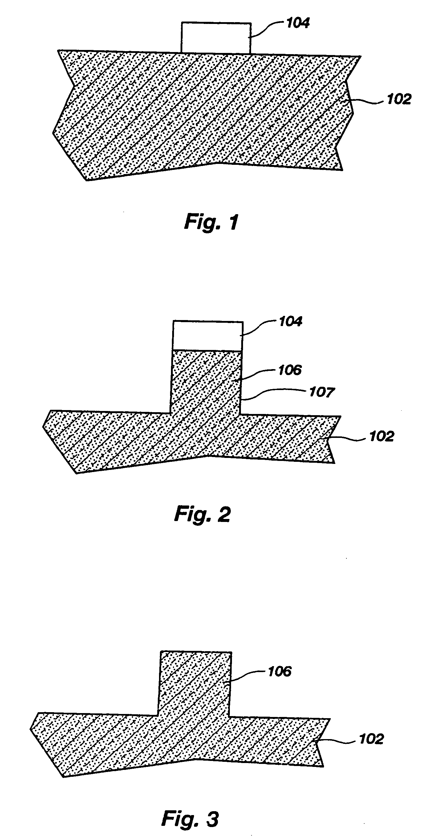
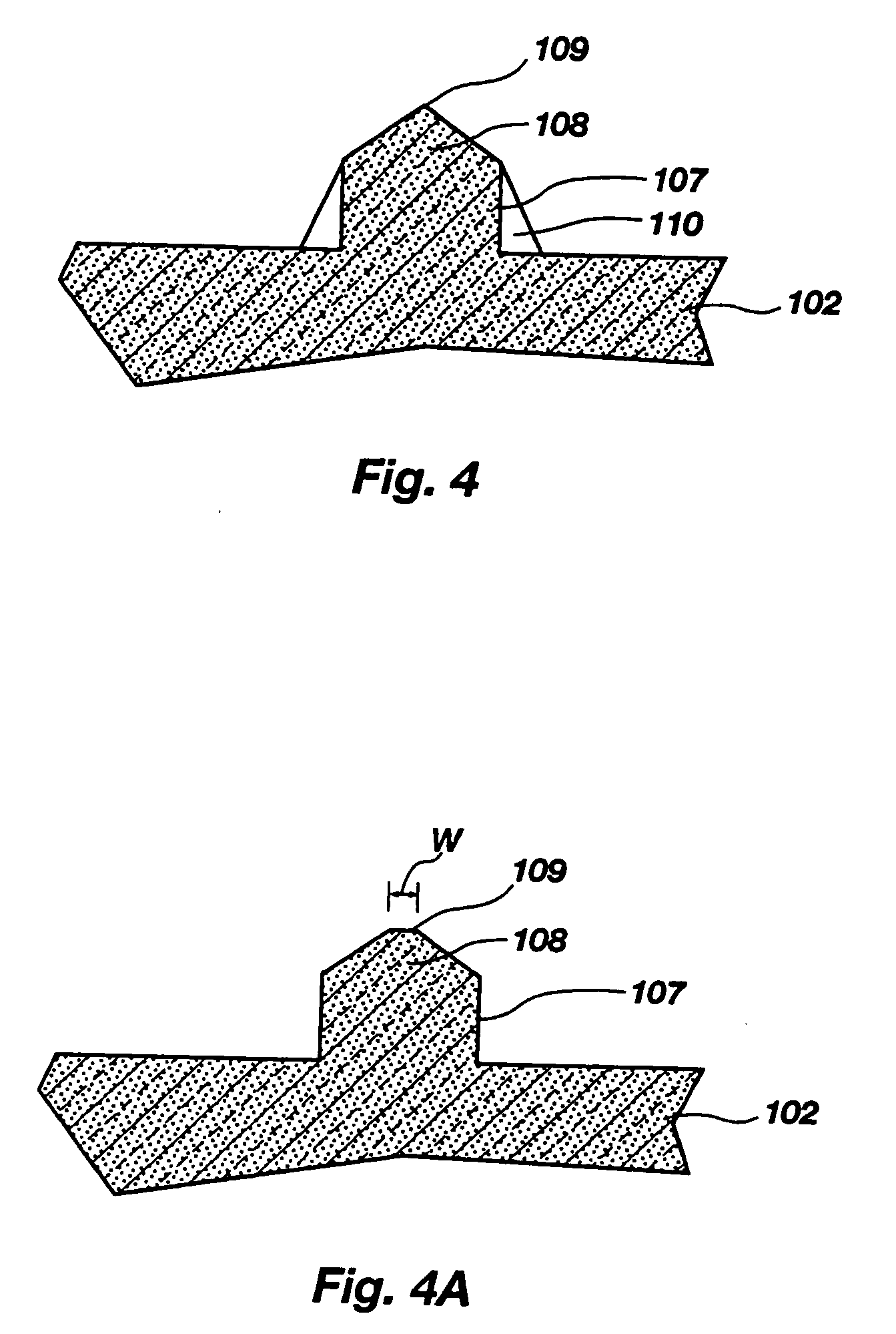
[0030]FIGS. 1-16 illustrate various methods of forming field emission tips according to the present invention. It should be understood that the illustrations are not meant to be actual views of any particular field emission device, but are merely idealized representations which are employed to more clearly and fully depict the formation of field emission tips of the present invention than would otherwise be possible. Additionally, elements common to FIGS. 1-16 retain the same numerical designation.

[0031]FIGS. 1-4 illustrate one embodiment for forming field emission tips according to the present invention. As shown in FIG. 1, an etch mask material, such as a photoresist material, is patterned by photolithography to define an etch mask element 104 on a substrate 102, such as a wafer of semiconductor material (e.g., silicon) or a silicon on insulator (SOI) type substrate, such as a silicon on glass (SOG) or silicon on sapphire (SOS) substrate. The substrate 102 may also be conductive ...


PUM


Abstract

A field emission tip includes a base with a central portion and a tapered portion. The central portion of the base includes a peripheral surface, at least a portion of which is oriented substantially vertically or perpendicularly relative to a plane in which a substrate from which the field emission tip protrudes resides. An apex may be located at an exposed end of the central portion of the base. The tapered portion of the base includes an inclined surface that extends toward the exposed end of the central portion of the base. The tapered portion of the base may be formed from material that is redeposited as the emission tip is fabricated. The apex may be formed, at least in part, from a low work function material, such as one or more of aluminum titanium silicide, titanium silicide nitride, titanium nitride, tri-chromium mono-silicon, and tantalum nitride. Field emission arrays and field emission displays that include such field emission tips are also disclosed.

Description

CROSS-REFERENCE TO RELATED APPLICATIONS [0001] This application is a continuation of application Ser. No. 09 / 939,848, filed Aug. 27, 2001, pending, which is a divisional of application Ser. No. 09 / 559,153, filed Apr. 26, 2000, now U.S. Pat. No. 6,387,717, issued May 14, 2002.BACKGROUND OF THE INVENTION [0002] 1. Field of the Invention [0003] The present invention relates to field emitters and methods of fabricating the same. More particularly, the present invention relates to forming field emission tips by the use of facet etching. [0004] 2. Background of Related Art [0005] Various types of field emitters are used in a variety of devices, from electron microscopes to ion guns. However, one of the most prevalent commercial applications of field emitters is flat panel displays, such as cold cathode field emission displays (“FEDs”) used for portable computers and other lightweight, portable information display devices. [0006] As illustrated in FIG. 18, an exemplary flat panel cold cath...

Claims


Application Information

Patent Timeline
Patent Type & Authority Applications(United States)
IPC IPC(8): H01J1/16H01J1/02H01J1/00H01J1/304
CPCH01J1/304H01J2201/30446H01J31/127H01J1/3044
Inventor BLALOCK, GUY T.TANG, SANH D.HUANG, ZHAOHUI
Owner BLALOCK GUY T
Why Eureka
Try Eureka