
Substrate processing apparatus and substrate processing method

a substrate processing and substrate technology, applied in the direction of coatings, chemical vapor deposition coatings, metallic material coating processes, etc., can solve the problem of difficult to deposit films with a sufficient thickness uniformity, and achieve uniform substrate processing. , the effect of reducing the resistance of process gas passing through the hol

Inactive Publication Date: 2006-11-23
PANASONIC CORP
View PDF4 Cites 4 Cited by
  • Summary
  • Abstract
  • Description
  • Claims
  • Application Information

AI Technical Summary

Benefits of technology

[0020] For a dry etching apparatus, an equivalent technique to thus improve the nonuniformity of reaction such as film formation by the single wafer type substrate processing apparatus is described in Document 2. This is the technique in which variation is produced in the diameters of the penetrating holes in order to ensure a uniform density of a reaction gas discharged from the entire surface of an electrode plate corresponding to the gas dispersion plate 17. To be more specific, the penetrating holes in the center of the electrode plate are made to have decreased diameters and those in the perimeter thereof are made to have increased diameters. According to this technique, appropriate setting of the diameter distribution of the penetrating holes can improve the etching uniformity (the value obtained by dividing the difference between the maximum and the minimum by the double of the average) to 3.3%.
[0056] As is apparent from the above, in the substrate processing apparatus of the present invention, the gas dispersion plate is designed so that the perimeter portion has a smaller thickness than the central portion and that the plurality of penetrating holes provided in the perimeter portion of the gas dispersion plate have a smaller length than the penetrating holes in the central portion thereof. With this, the flow rate of the process gas discharged from the plurality of penetrating holes toward the substrate can be made uniform with a higher accuracy than the conventional technique. As a result of this, the uniformity of substrate processing over the substrate surface can be improved more than the conventional technique. This uniformly carries out, for example, dry etching, plasma etching, film formation, and the like, so that the present invention is useful in fabricating a product such as a semiconductor integrated circuit.

Problems solved by technology

This makes it difficult to deposit a film with a sufficient thickness uniformity for the purpose of fabricating the semiconductor integrated circuit device with a high yield.

Method used


Image

  • Substrate processing apparatus and substrate processing method
  • Substrate processing apparatus and substrate processing method
  • Substrate processing apparatus and substrate processing method

Examples


first embodiment

[0062] Hereinafter, a substrate processing apparatus according to a first embodiment of the present invention will be described with reference to the accompanying drawings.

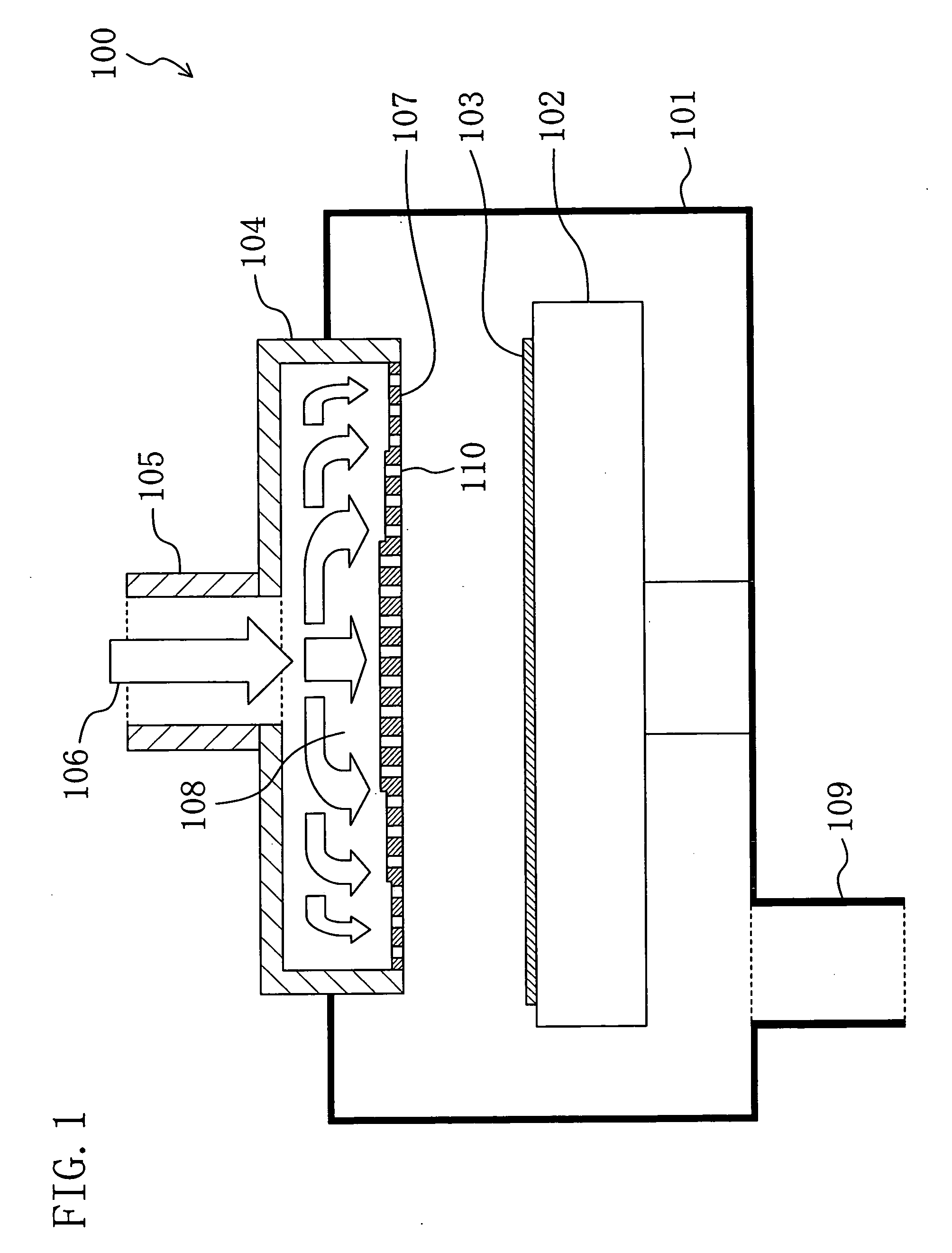
[0063]FIG. 1 is a sectional view schematically showing the inner structre of a substrate processing apparatus, more specifically, a chemical vapor deposition apparatus 100 according to the first embodiment of the present invention, which is used to fabricate a semiconductor integrated circuit. The chemical vapor deposition apparatus 100 of the first embodiment and the conventional chemical vapor deposition apparatus 10 shown in FIG. 5A differ in the shape of a gas dispersion plate provided in a shower head. Detailed description of this will be made below.

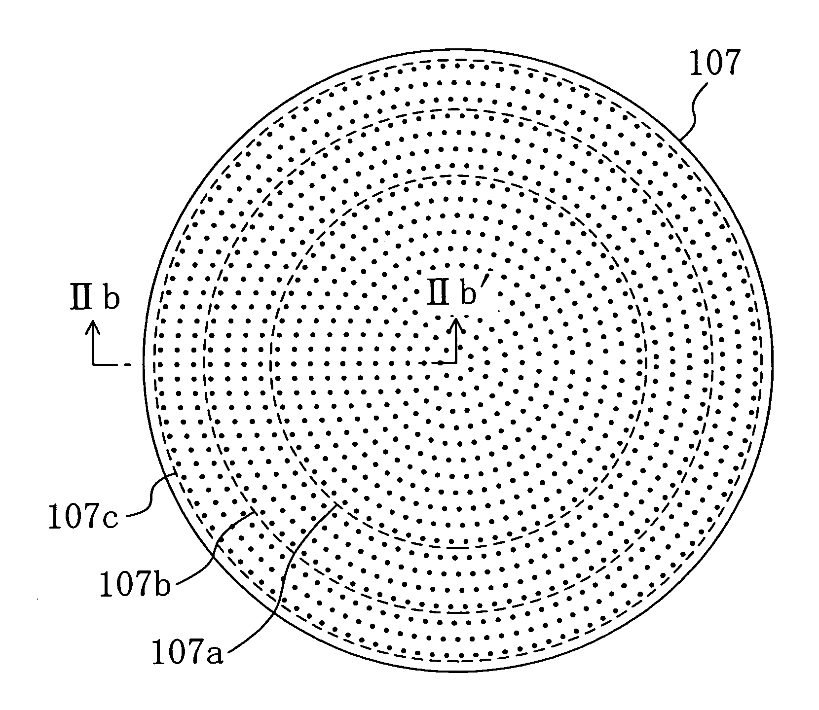
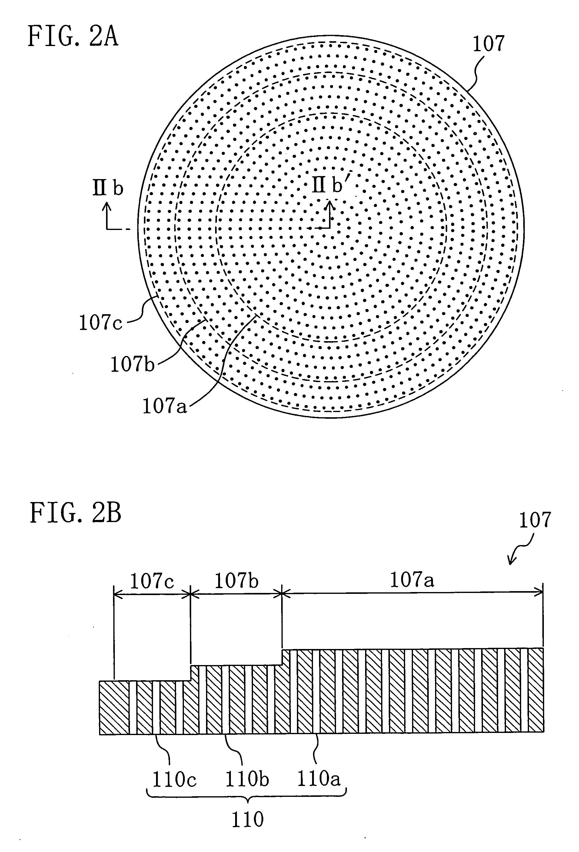
[0064] The chemical vapor deposition apparatus 100 has a pedestal 102 provided in a reaction chamber 101 within which a film is grown, and a substrate 103 to be processed is placed on the pedestal 102. In an upper portion of the reaction chamber 101, a shower he...

second embodiment

[0096] Next, a substrate processing apparatus according to a second embodiment of the present invention will be described with reference to the accompanying drawings.

[0097]FIG. 4 is a sectional view schematically showing the inner structre of a substrate processing apparatus, more specifically, a chemical vapor deposition apparatus 200 according to the second embodiment of the present invention, which is used to fabricate a semiconductor integrated circuit.

[0098] The chemical vapor deposition apparatus 200 has the structure in which a second shower head 204 and a second gas dispersion plate 207 are added to the chemical vapor deposition apparatus 100 of the first embodiment. Thus, the description of the components of the chemical vapor deposition apparatus 200 shown in FIG. 4 that are the same as those of the chemical vapor deposition apparatus 100 of the first embodiment will be omitted by retaining the same reference numerals as FIG. 1.

[0099] Referring to FIG. 4, the chemical v...


PUM

PropertyMeasurementUnit
Lengthaaaaaaaaaa
Thicknessaaaaaaaaaa
Shapeaaaaaaaaaa

Abstract

A substrate processing apparatus comprises: a reaction chamber for processing a substrate using a process gas; a pedestal provided in the reaction chamber and placing the substrate; and a shower head for introducing the process gas into the reaction chamber. The shower head includes a gas dispersion plate which is formed with a plurality of penetrating holes for diffusing the process gas and is provided to face the pedestal. The gas dispersion plate includes a central portion and a perimeter portion having a smaller thickness than the central portion, and the ones of the plurality of penetrating holes provided in the perimeter portion have a smaller length than the ones of the plurality of penetrating holes provided in the central portion.

Description

CROSS-REFERENCE TO RELATED APPLICATIONS [0001] This application claims priority under 35 U.S.C. §119 on Patent Application No. 2005-148715 filed in Japan on May 20, 2005, the entire contents of which are hereby incorporated by reference. BACKGROUND OF THE INVENTION [0002] (a) Fields of the Invention [0003] The present invention relates to substrate processing apparatuses and substrate processing methods. In particular, the present invention relates to substrate processing apparatuses and substrate processing methods capable of improving the uniformity of processing such as film formation or etching. [0004] (b) Description of Related Art [0005] In recent years, there has been a growing trend in semiconductor integrated circuit devices toward a larger packing density and a lower power consumption, while manufacturing costs of the devices have increasingly dropped due to enlargement of diameter of a semiconductor substrate or other approaches. In order to simultaneously attain miniatur...

Claims


Application Information

Patent Timeline
IPC IPC(8): C23F1/00C23C16/00
CPCH01L21/67069C23C16/45565
Inventor UEDA, SATOSHINAKAJIMA, TAMAKI
Owner PANASONIC CORP
Learn More