
Protection circuit module for a secondary battery and a battery package using same

a protection circuit module and battery technology, applied in secondary cell servicing/maintenance, cell components, cell component details, etc., can solve the problems of high cost, inability to reduce resistance, use gold, etc., to reduce the area of the wiring board, reduce the cost, and reduce the size of the protection circuit module

Inactive Publication Date: 2006-11-16
RICOH ELECTRONIC DEVICES CO LTD
View PDF3 Cites 26 Cited by
  • Summary
  • Abstract
  • Description
  • Claims
  • Application Information

AI Technical Summary

Benefits of technology

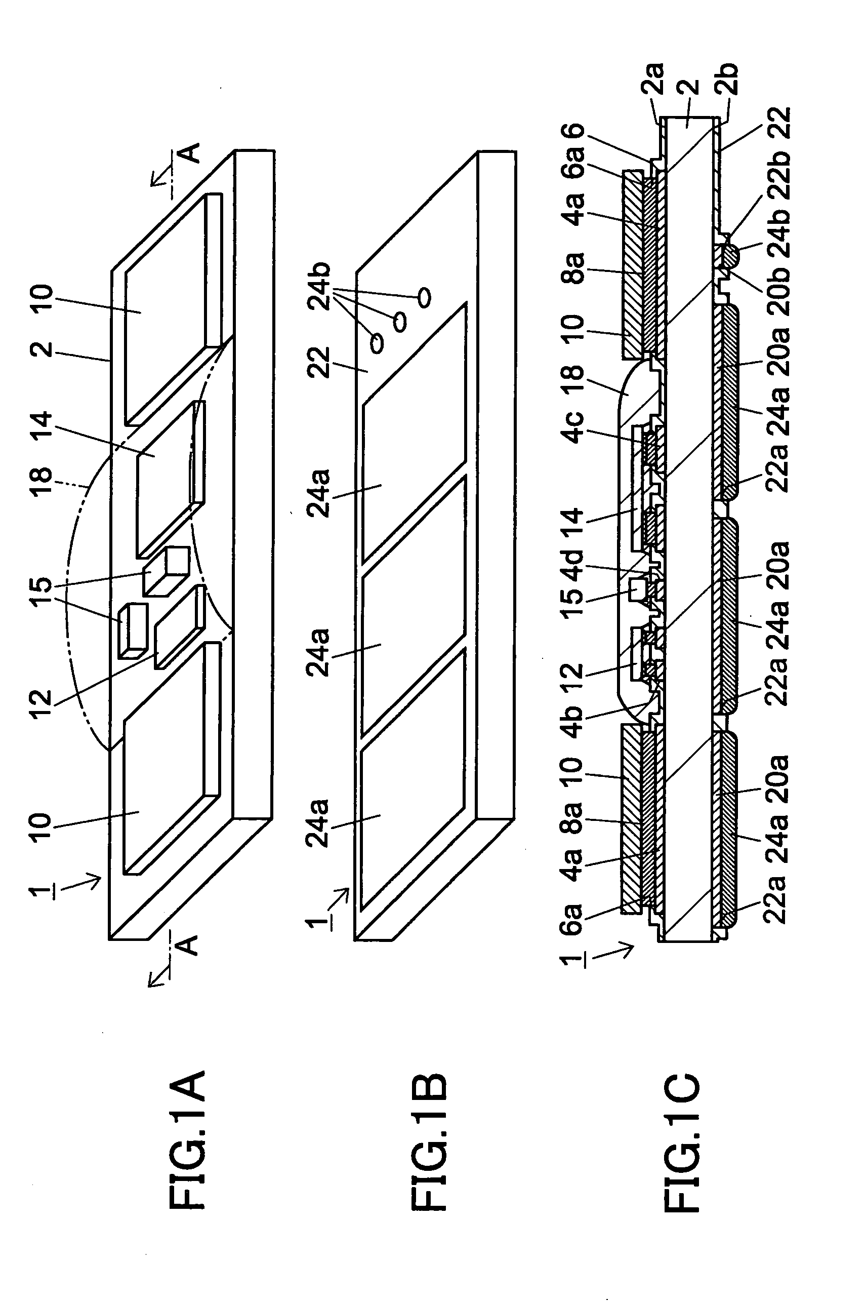
[0032] In the protection circuit module for a secondary battery of the present invention, on a wiring board, battery-side external terminals are disposed on one surface, and load-side external terminals are disposed on a surface on the opposite side. Accordingly, compared with the case where the load-side external terminals and the battery-side external terminals are disposed on the same surface of the wiring board, it is possible to reduce the area of the wiring board, so that it is possible to realize downsizing of the protection circuit module. Further, semiconductor components are mounted face-down on the wiring board. Accordingly, compared with the case of employing wire bonding, it is possible to realize cost reduction and reduce the mounting area of the semiconductor components. Thus, according to the protection circuit module for a secondary battery of the present invention, it is possible to realize reduction in the size and cost of the protection circuit module.
[0033] In the protection circuit module of the present invention, the semiconductor components may be a protection IC chip and a field effect transistor chip. This makes it possible to reduce the ON resistance of the field effect transistor since the field effect transistor chip is mounted face-down.
[0034] Further, the semiconductor components may be covered with sealing resin. This makes it possible to protect the semiconductor components.
[0035] Further, an insulating material layer having openings corresponding to at least the external connection terminals of the semiconductor components and the battery-side external terminals may be formed on the one surface of the wiring board, and the semiconductor components may be mounted on the wiring board through solder formed in the openings. This makes it possible to interpose the insulating material layer between the adjacent external connection terminals of the semiconductor components, thus making it possible to prevent short-circuiting between the adjacent external connection terminals.
[0036] Further, nickel plates may be disposed on the battery-side external terminals through solder. This makes it possible to connect an interconnection member for electrically connecting the secondary battery and the battery-side external terminals to the metal plates.
[0037] Further, in the protection circuit module of the present invention, a gold plating layer may be formed on the surface of the load-side external terminals. This makes it possible to stabilize the electrical connection between the terminals of a load such as a portable apparatus or a charger and the load-side external terminals of the protection circuit module.

Problems solved by technology

However, it has been a problem that the package product, in which semiconductor chips and lead terminals are connected with bonding wires, causes an increase in cost.
Further, it has been a problem that in the current control transistors 54 and 56, in which semiconductor chips are electrically connected to the wiring board through bonding wires and lead terminals, it is impossible to reduce ON resistance.
However, gold, which is costly, is used as the material of the bonding wires.
Accordingly, it has been a problem that there is a limit to cost reduction.
Further, it has been a problem that in current control transistors, in which semiconductor chips are electrically connected to the wiring board through bonding wires, it is impossible to reduce ON resistance.

Method used


Image

  • Protection circuit module for a secondary battery and a battery package using same
  • Protection circuit module for a secondary battery and a battery package using same
  • Protection circuit module for a secondary battery and a battery package using same

Examples


Embodiment Construction

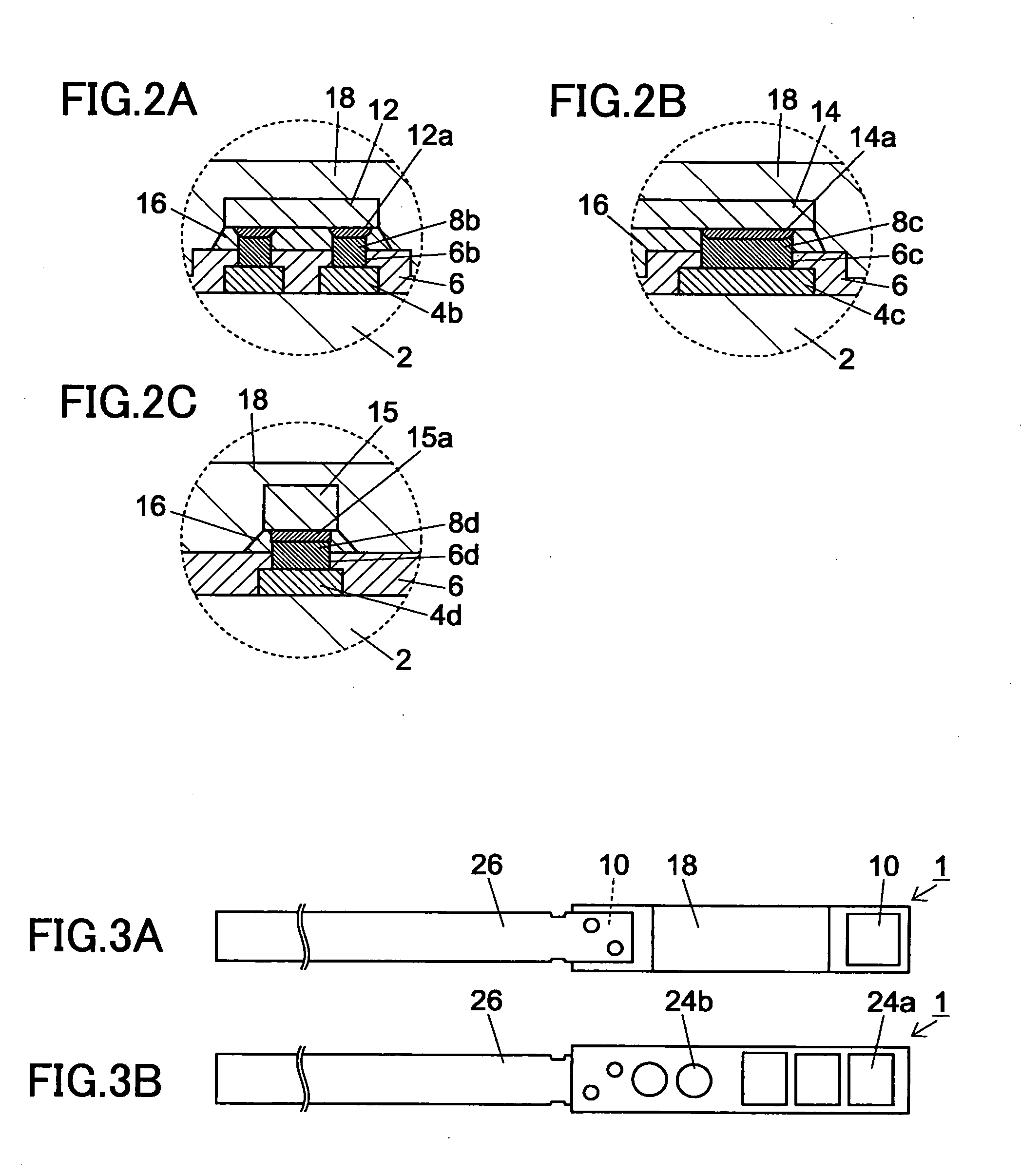
[0043]FIG. 1 is schematic diagrams showing an embodiment of a protection circuit module. (A) is a schematic perspective view on the side of a surface, (B) is a schematic perspective view on the bottom surface side, and (C) is a cross-sectional view at the A-A position of (A). FIG. 2(A) is a cross-sectional view showing the vicinity of the mounting area of a protection IC chip at greater magnification. FIG. 2(B) is a cross-sectional view showing the vicinity of the mounting area of a field effect transistor chip at greater magnification. FIG. 2(C) is a cross-sectional view showing the vicinity of the mounting area of an electronic component at greater magnification. A description is given of this embodiment referring to FIGS. 1 and 2.

[0044] A protection circuit module 1 has a wiring board 2. Two battery-side external terminals 4a, multiple electrodes 4b for a protection IC chip, multiple electrodes 4c for a field effect transistor chip, multiple electrodes 4d for an electronic compo...


PUM


Abstract

To realize reduction in the size and cost of a protection circuit module for a secondary battery. A protection circuit module 1 for a secondary battery has at least a wiring board 2 having multiple battery-side external terminals 4a and multiple load-side external terminals 20a, and semiconductor components 12 and 14 mounted on the wiring board 2. On the wiring board 2, the battery-side external terminals 4a are disposed on a surface 2a, and the load-side external terminals 20a are disposed on a surface 2b on the opposite side. The semiconductor components 12 and 14 have multiple external connection terminals 12a and 14a arranged on a single plane surface, and are mounted face-down in a bare-chip state on the surface 2a of the wiring board 2.

Description

BACKGROUND OF THE INVENTION [0001] 1. Technical Field [0002] The present invention relates to a protection circuit module for a secondary battery and a battery package using the same. [0003] 2. Background Art [0004] Secondary batteries, which can be charged and discharged repeatedly, are often used as batteries to be mounted in a variety of portable information apparatuses. Prevention of degradation of, supplying power for a long period of time to, downsizing of, and inexpensiveness of secondary batteries are considered important. Conventionally, for instance, battery packages of a lithium ion battery have a built-in protection circuit module in which is mounted a protection circuit for preventing the battery from being degraded by excessive heat generation due to an overcurrent caused to flow by short-circuiting of an electric circuit or incorrect charging (a large voltage or reverse voltage). [0005] For instance, there is a protection circuit that has a transistor for current cont...

Claims


Application Information

Patent Timeline
IPC IPC(8): H01M2/34H02H7/00H01M50/586
CPCH01M2/34H05K1/181H01M10/425Y02E60/10H01M50/586
Inventor TAN, KUNIHIROHIGASHIGUCHI, MASAHIROMORISHITA, SEIICHIMITSUKE, YUKIYOSHI
Owner RICOH ELECTRONIC DEVICES CO LTD
Learn More