Electro-optical device and method for manufacturing the same
a technology of optical devices and optics, applied in the field of electric devices, can solve the problems of large area required in the connection portion, inability to apply to a high-resolution display, and wire connection problems
- Summary
- Abstract
- Description
- Claims
- Application Information
AI Technical Summary
Benefits of technology
Problems solved by technology
Method used
Image
Examples
embodiment 1
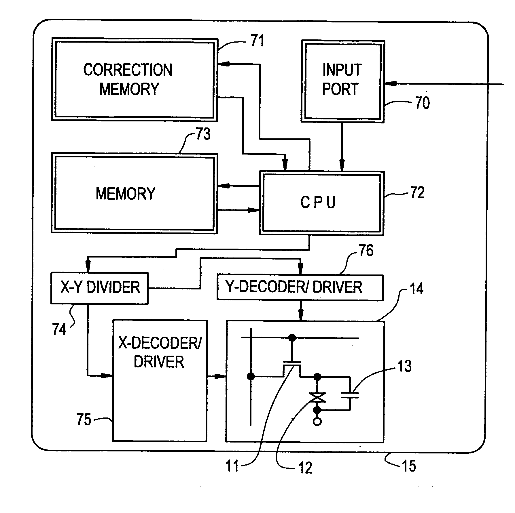
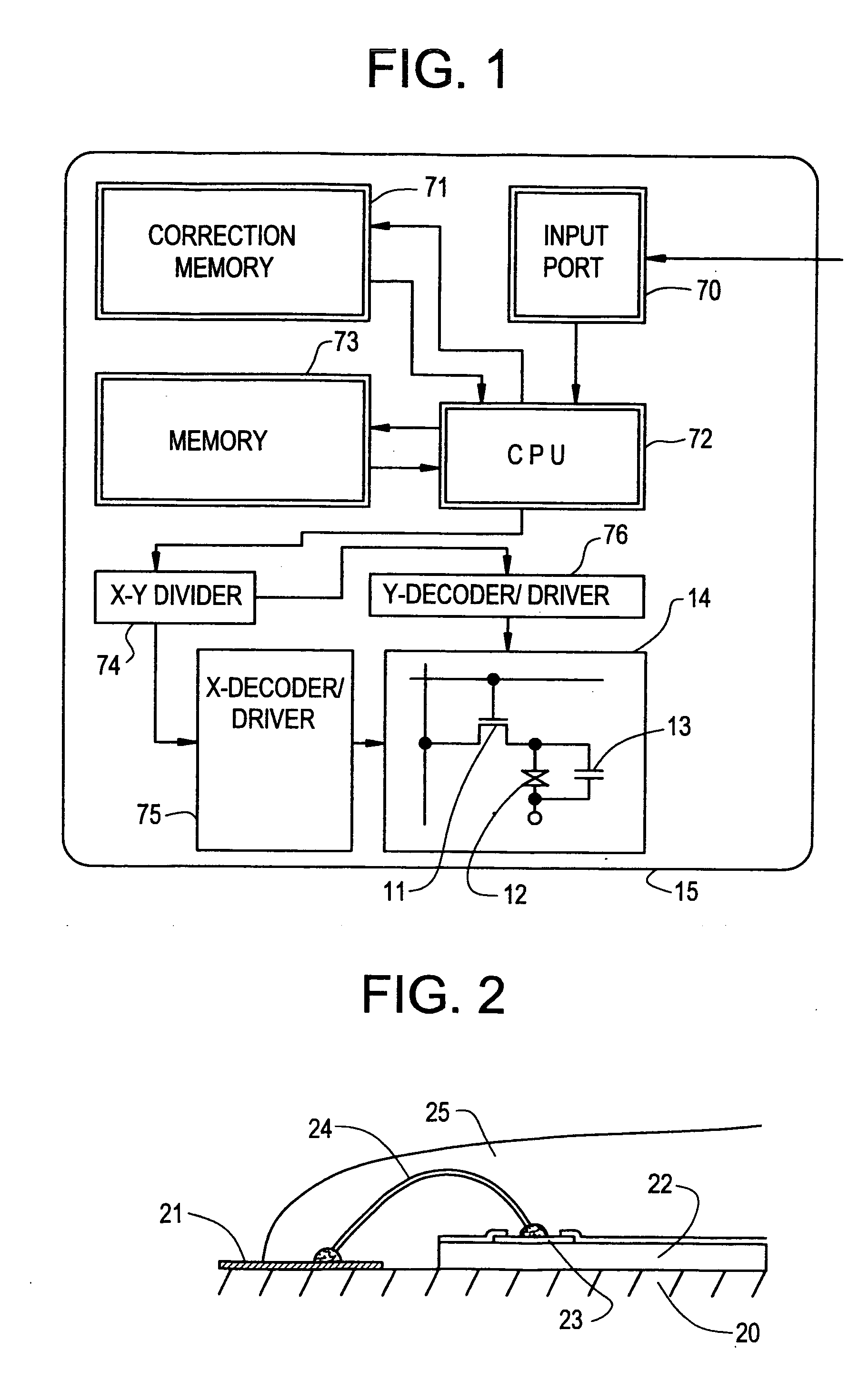
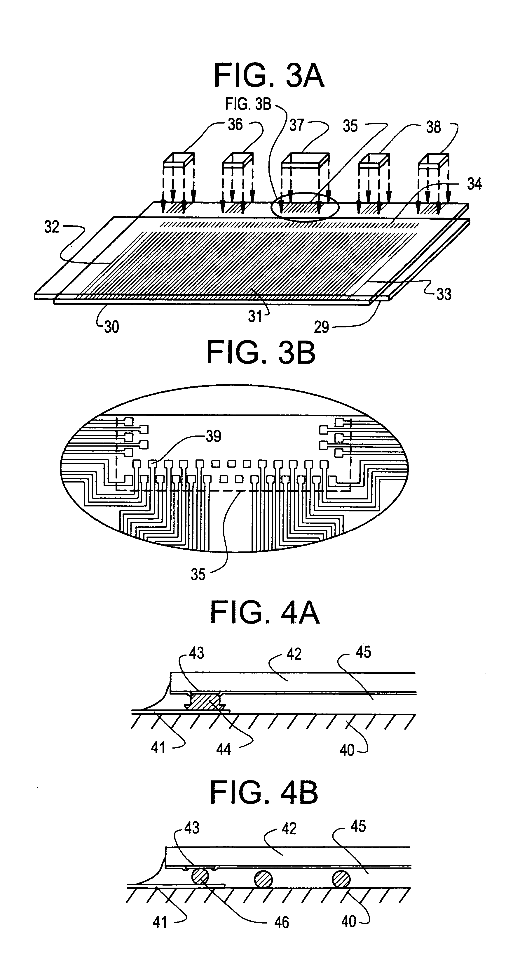
[0025]FIG. 3 shows a schematic view of a liquid crystal display panel according to an embodiment of the present invention. In FIG. 3, a substrate (board) 29 is placed opposite to the substrate (board) 30 and a liquid crystal material is held between the substrates 29 and 30. An active matrix circuit 31 and peripheral driving circuits 32 to 34 for driving the active matrix circuit 31 are formed using thin film transistors (TFTs) on the substrate 30 such as a glass substrate. Also, main memory chips 36, MPU (microprocessing unit) 37 or CPU (central processing unit) and correction memories 38 are adhered to a surface of the substrate 30 in which the above circuits 31 to 34 are formed, and electrically connected with the above circuits 31 to 34. For example, when chips are connected with a substrate by a FCOG, a wiring terminal portion (wiring connection pad) 39 (corresponding to a wiring portion 41 of FIGS. 4A and 4B) made of the ITO are formed in a portion 35 of the substrate 30.
[002...
embodiment 2
[0029] A panel as shown in FIG. 3 is manufactured. The active matrix circuit 31 and the peripheral driving circuits 32 to 34 are formed using TFTs on the substrate 30. The main memory chips 36, the MPU (microprocessing unit) 37 or CPU (central processing unit) and the correction memories 38 are adhered to a surface of the substrate 30 in which the above circuits 31 to 34 are formed, and electrically connected with the wiring terminal portion (wiring connection pad) 39 (corresponding to the terminal electrode 21) which is made of an aluminum alloy thin film and formed on the substrate 40 by a wire bonding as shown in FIG. 2. A gold fine line is used as a bonding wire
embodiment 3
[0030] In this embodiment, chips are adhered to a TFT circuit (monolithic type active matrix circuit) substrate by a FCOG, to construct further improved circuit. A process for manufacturing a monolithic type active matrix circuit will be described later using FIGS. 5A to 5G. A silicon oxide film having a thickness of 1000 to 3000 Å is formed as a base oxide film 502 on a substrate (Corning 7059) 501. A method for forming this oxide film may include a sputtering in an atmosphere containing oxygen or a plasma CVD (Chemical Vapor Deposition).
[0031] A silicon film having amorphous or crystalline is formed at a thickness of 300 to 1500 Å, preferably 500 to 1000 Åby a plasma CVD or a low pressure CVD (LPCVD). In order to form an crystalline silicon film, after forming an amorphous silicon film, a laser or an intense light equivalent to the laser may be irradiated (light annealing), or thermal annealing may be performed at 500° C. or higher for a long time of period. Also, after crystalli...
PUM
| Property | Measurement | Unit |
|---|---|---|
| thickness | aaaaa | aaaaa |
| sheet resistance | aaaaa | aaaaa |
| temperature | aaaaa | aaaaa |
Abstract
Description
Claims
Application Information
 - R&D
- Intellectual Property
- Life Sciences
- Materials
- Tech Scout
- Unparalleled Data Quality
- Higher Quality Content
- 60% Fewer Hallucinations
Browse by: Latest US Patents, China's latest patents, Technical Efficacy Thesaurus, Application Domain, Technology Topic, Popular Technical Reports.
© 2025 PatSnap. All rights reserved.Legal|Privacy policy|Modern Slavery Act Transparency Statement|Sitemap|About US| Contact US: help@patsnap.com


