
Method for manufacturing a laminate cover, laminate protective layer, and laminate electronic device having a reduced cost, manufacturing time, weight, and thickness

Inactive Publication Date: 2006-11-09
NOKIA CORP
View PDF44 Cites 18 Cited by
  • Summary
  • Abstract
  • Description
  • Claims
  • Application Information

AI Technical Summary

Benefits of technology

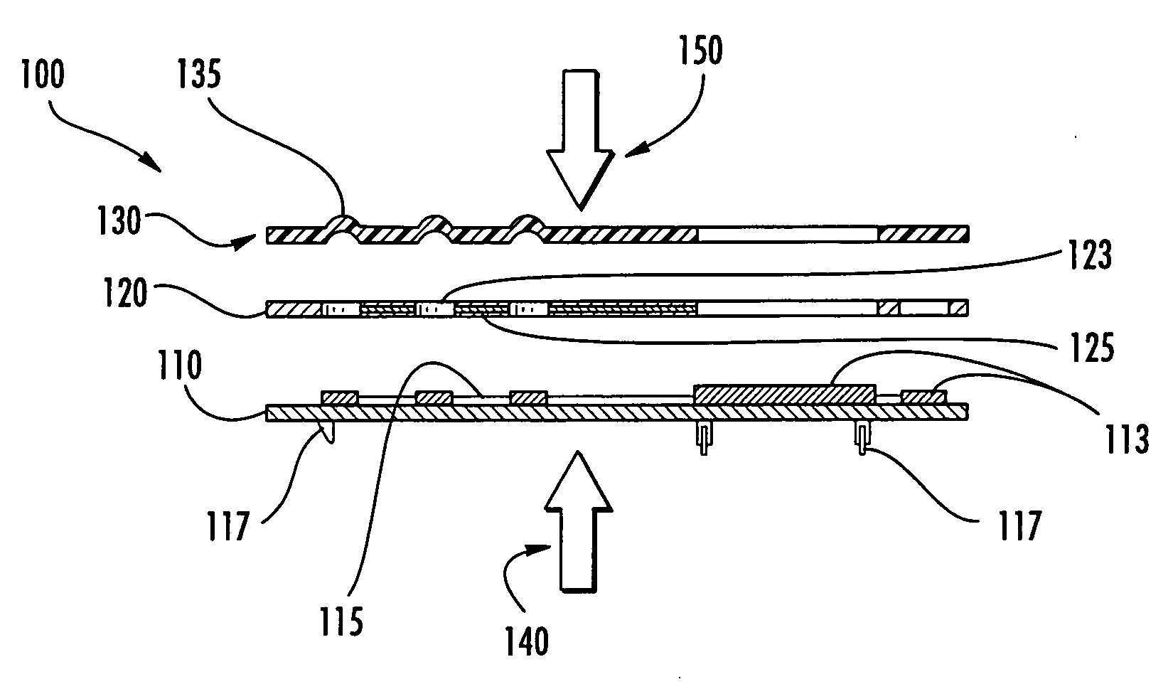
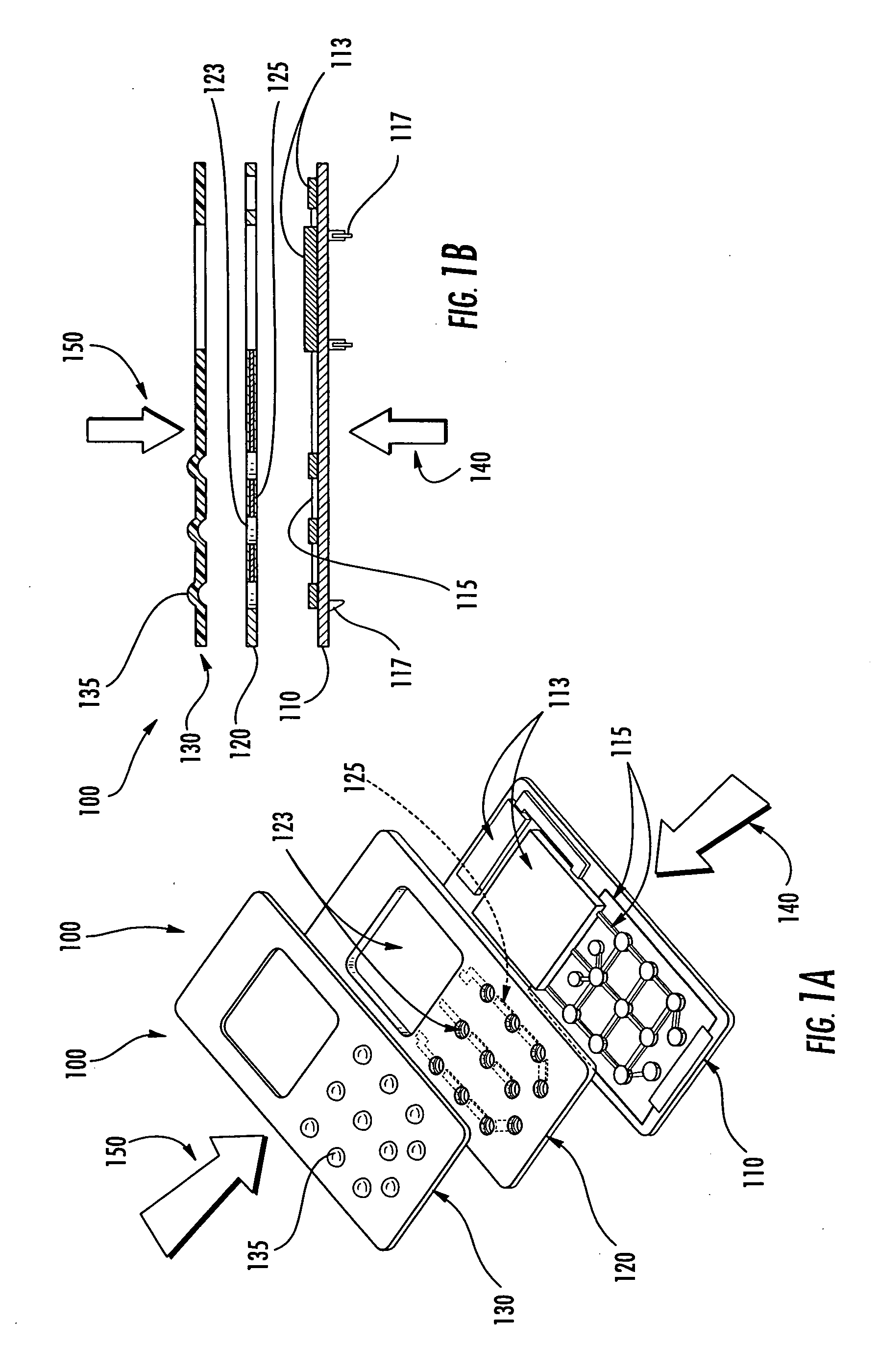
[0006] The above and other needs are met by the present invention which, in various embodiments, provides various methods for manufacturing a cover, protective layer, and / or an entire electronic device having a laminate structure wherein electronic components are at least partially embedded within the electronic device, and / or within the cover or protective layer used to encase and / or support an electronic device so as to reduce the overall weight and thickness of the electronic device. According to one embodiment, the method for manufacturing the electronic device (or multimedia device, for example) comprises the steps of attaching at least one electronic component to one side of a first support layer such that a conductive portion of the electronic component is capable of communicating with the multimedia device, applying an adhesive layer to the first support layer, and applying a second support layer to the adhesive layer so as to laminate the at least one electronic component between the first and second support layers to form the electronic device and / or the protective cover or layer for an electronic device. Thus, the method may, in some embodiments, be used to manufacture a laminate layer or other laminate component that is adapted to be capable of operably engaging an electronic device such that the at least one electronic component is capable of communicating with the electronic device via the conductive portion.
[0008] Another embodiment of the present invention provides a method for manufacturing a layer, cover, or other laminate component of an electronic device wherein the components of the layer are advanced, aligned, and selectively laminated together so as to allow the efficient manufacture thereof. Such an embodiment first comprises advancing a first support layer in a first direction wherein the first support layer has at least one electronic component attached to one side thereof such that a conductive portion of the electronic component is capable of communicating with the electronic device, and wherein the first support layer also has an adhesive layer operably engaged with at least a portion of one side of the first support layer. This method also comprises the steps of advancing a second support layer in a direction substantially perpendicular to the first direction such that the second support layer is substantially adjacent to the side of the first support layer having the at least one electronic component attached, and selectively laminating the at least one electronic component between the first and second support layers to form the layer. According to this embodiment, the layer may also be adapted to be capable of operably engaging the electronic device such that the at least one electronic component is capable of communicating with the electronic device via the at least one conductive portion. In addition, such an embodiment provides for the continuous production of such layers by advancing the support layers in a continuous reel (as sub-assemblies) and selectively laminating the support layers together to form layers that may be trimmed off from the continuous assembly line.
[0009] In another embodiment, the present invention provides a method of manufacturing a layer or other component of an electronic device using injection molding techniques with the layer having at least one electronic component and / or conductive elements integrated therein. The manufacturing method of this embodiment comprises the steps of placing at least one electronic component on one side of a first carrier layer such that at least one conductive portion of the at least one electronic component is adapted to be capable of communicating with the electronic device, positioning a second carrier layer adjacent to the first carrier layer so as to support the at least one electronic component between the first and second carrier layers and to form a mold for the layer, injecting a molten polymer between the first and second carrier layers, hardening the polymer such that the layer is formed between the first and second carrier layers, and removing the first and second carrier layers from the layer. Thus, the layer formed in this process is capable of operably engaging the electronic device such that the at least one electronic component is capable of communicating with the electronic device via the at least one conductive portion.
[0011] Thus the various method embodiments for manufacturing a cover, protective layer, and / or electronic device of the present invention provide many advantages that may include, but are not limited to: providing a rapid and / or low-cost manufacturing method for producing a cover, protective layer, and / or electronic device having a reduced weight and thickness, providing a method for sealing and / or enclosing an electronic device (such as a multimedia device) with a robust, flexible, covering that may effectively seal the electronic device while providing a number of electronic functions therein; manufacturing a cover, protective layer, and / or electronic device having integrated user-interface capabilities including integrated keypad switches, integrated light-guides, integrated RFID components, and other electronic components that may be in communication with the transmitter, receiver, display, and / or other electronic devices within the electronic device, and providing a method that may be used to cost-effectively customize existing electronic devices at a point-of-sale so as to add additional electronic functions and / or decorative personalization features to the electronic device at a site that is remote from the point of electronic device manufacturing.

Problems solved by technology

The basic mechanical structure, however, of most multimedia devices, such as, for instance a mobile terminal, has not changed considerably in recent years, thereby limiting the reduction in size and weight of multimedia devices.
The outer casing of such conventional electronic devices, however, is designed only to enclose and protect the electronic components and / or circuit boards supported therein, and does not provide for additional functionality.
Thus, such conventional devices must bear the weight and size penalty of providing all of the functional electronic components as well as the separate structural casing components used to enclose and support the electronic components.
This, in turn results in the casing having increased weight and thickness.

Method used


Image

  • Method for manufacturing a laminate cover, laminate protective layer, and laminate electronic device having a reduced cost, manufacturing time, weight, and thickness
  • Method for manufacturing a laminate cover, laminate protective layer, and laminate electronic device having a reduced cost, manufacturing time, weight, and thickness
  • Method for manufacturing a laminate cover, laminate protective layer, and laminate electronic device having a reduced cost, manufacturing time, weight, and thickness

Examples


Embodiment Construction

)

[0020] The present invention now will be described more fully hereinafter with reference to the accompanying drawings, in which preferred embodiments of the invention are shown. This invention may, however, be embodied in many different forms and should not be construed as limited to the embodiments set forth herein; rather, these embodiments are provided so that this disclosure will be thorough and complete, and will fully convey the scope of the invention to those skilled in the art. Like numbers refer to like elements throughout.

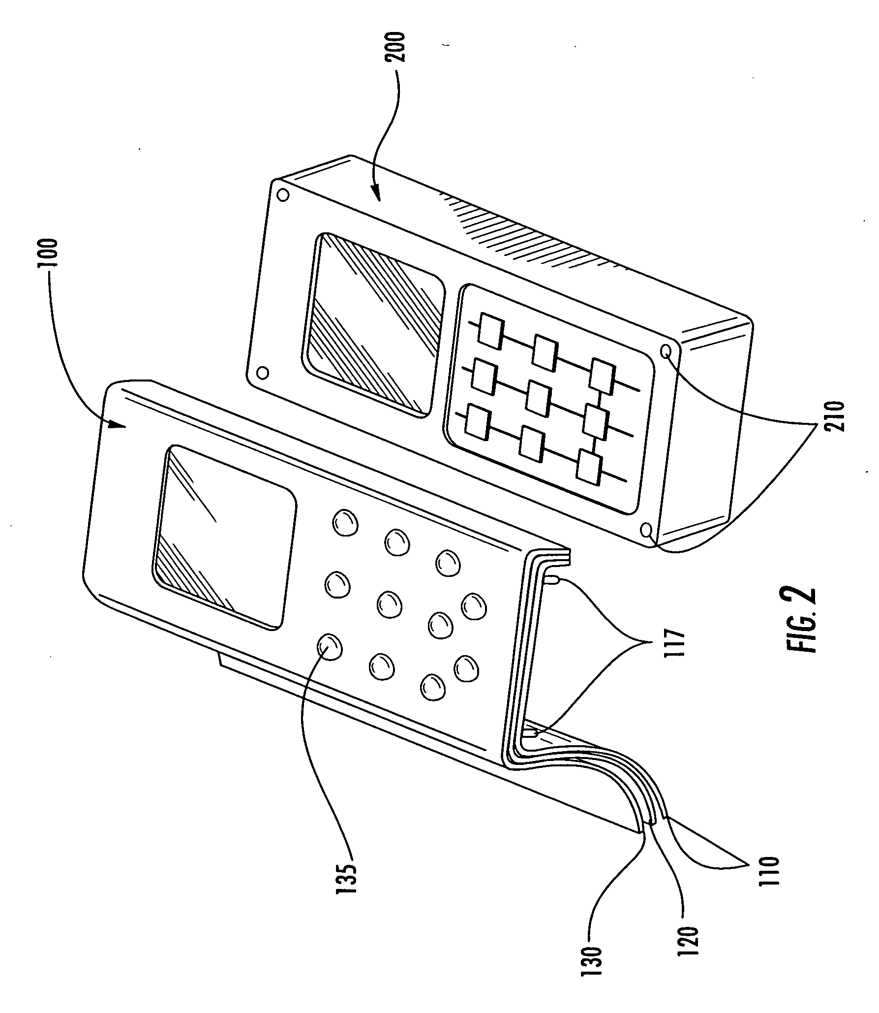
[0021] While the methods for manufacturing a cover, protective layer, and / or electronic device are described below in the context of a layer 100 operably engaged with a multimedia device 200 (such as a mobile terminal 200), it should be understood that the embodiments of the present invention may also be utilized to efficiently manufacture a layer 100 and / or protective layer configured to protect, support, and add electronic functionality to a variety o...


PUM

PropertyMeasurementUnit
Temperatureaaaaaaaaaa
Flexibilityaaaaaaaaaa
Electrical conductoraaaaaaaaaa

Abstract

A method is provided for manufacturing an electronically functional structural component adapted to integrate a plurality of electronic functions into a laminate cover, layer, and / or laminate component, for protecting, supporting, and / or forming a complete electronic device (such as a multimedia device). The method includes laminating a plurality of structural and / or protective layers interspersed with electronically functional layers or electronic components in communication with the multimedia device to form a supportive and electronically functional layer, cover, protective layer, and / or electronic device. Thus, the manufacturing methods provided allow for the cost-effective addition of thin and lightweight functional, protective, and / or decorative layers to a multimedia device or other electronic device at a sales location or other customization location.

Description

FIELD OF THE INVENTION [0001] The present invention relates generally to the manufacture of mechanical and electronic structures of electronic devices such as multimedia devices and, more particularly, relates to a method for manufacturing covers, structural components, engines, and / or other components of electronic devices wherein electronic connections and conduits are integrated with laminated structures. BACKGROUND OF THE INVENTION [0002] Modern electronic devices have become more miniaturized as electronic components such as integrated circuits have been decreased in size while having augmented processing power, memory capability, and cooling characteristics. The basic mechanical structure, however, of most multimedia devices, such as, for instance a mobile terminal, has not changed considerably in recent years, thereby limiting the reduction in size and weight of multimedia devices. [0003] For instance, conventional multimedia devices, such as mobile terminals, generally compr...

Claims


Application Information

Patent Timeline
IPC IPC(8): B32B37/00
CPCH01H2207/014Y10T29/49165H01H2209/06H01H2221/002H01H2229/004H01H2229/022H01H2229/028H01H2229/03H01H2229/05H01H2239/01H04M1/0283H04M1/23Y10T29/49124Y10T29/4913Y10T29/49117Y10T29/49144Y10T29/49126H01H2207/026H05K1/18H05K3/30
Inventor VATANPARAST, RAMINAARRAS, MIKKODUNFORD, STEVEN O.FUJII, TAKAHARULAINONEN, JUHANINOUSIAINEN, JAAKKORANTALA, JUKKA I.TANSKANEN, PIAYAMAMOTO, TETSUYA
Owner NOKIA CORP
Learn More