
All-reflective optical systems for broadband wafer inspection

a technology of optical systems and optical systems, applied in the direction of optical radiation measurement, photometry using electric radiation detectors, instruments, etc., can solve the problems of affecting the detection of defects of decreasing size, etc., to achieve low central obscuration and low distortion

Active Publication Date: 2006-10-05
KLA TENCOR TECH CORP
View PDF13 Cites 44 Cited by
  • Summary
  • Abstract
  • Description
  • Claims
  • Application Information

AI Technical Summary

Benefits of technology

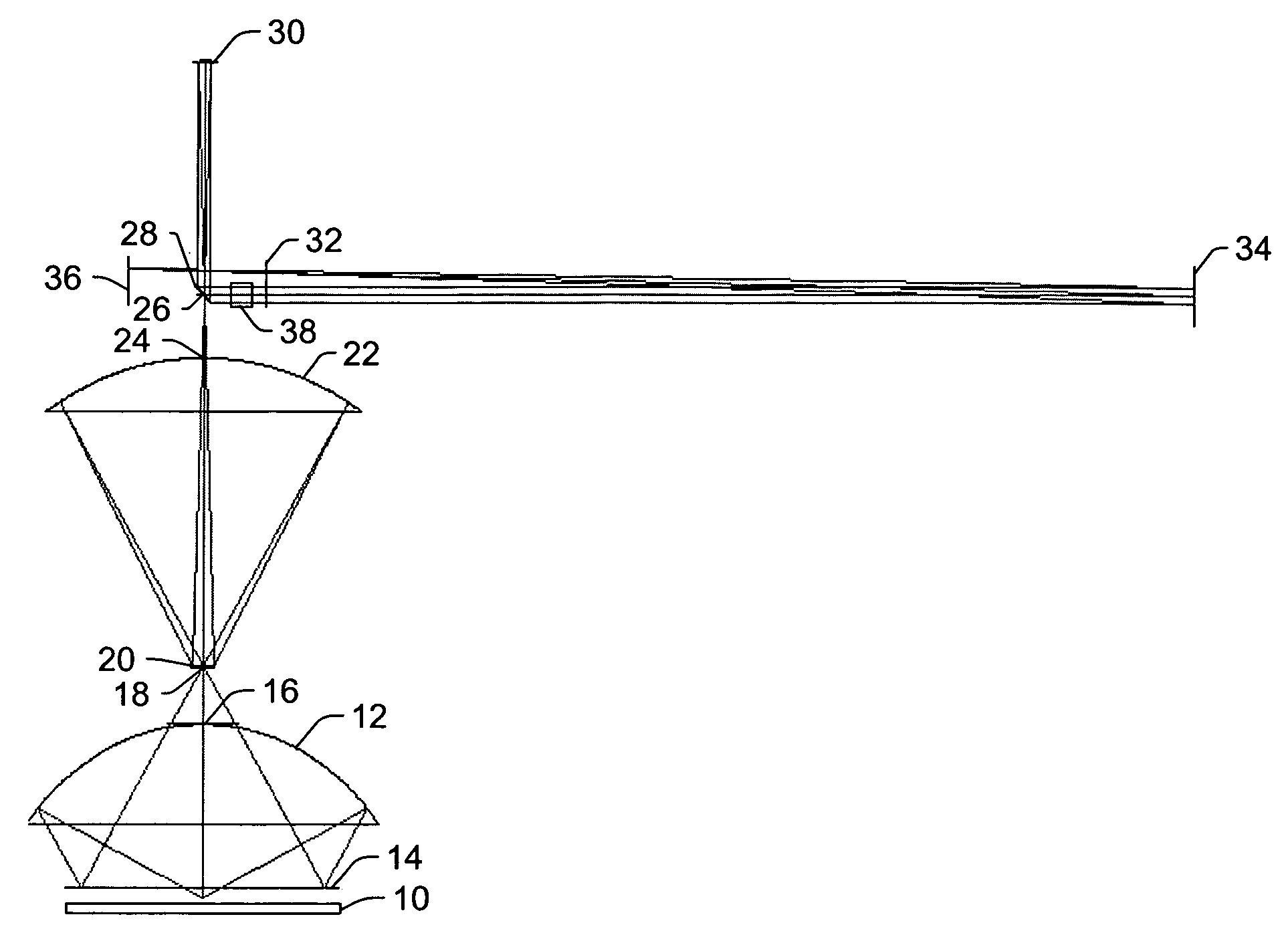
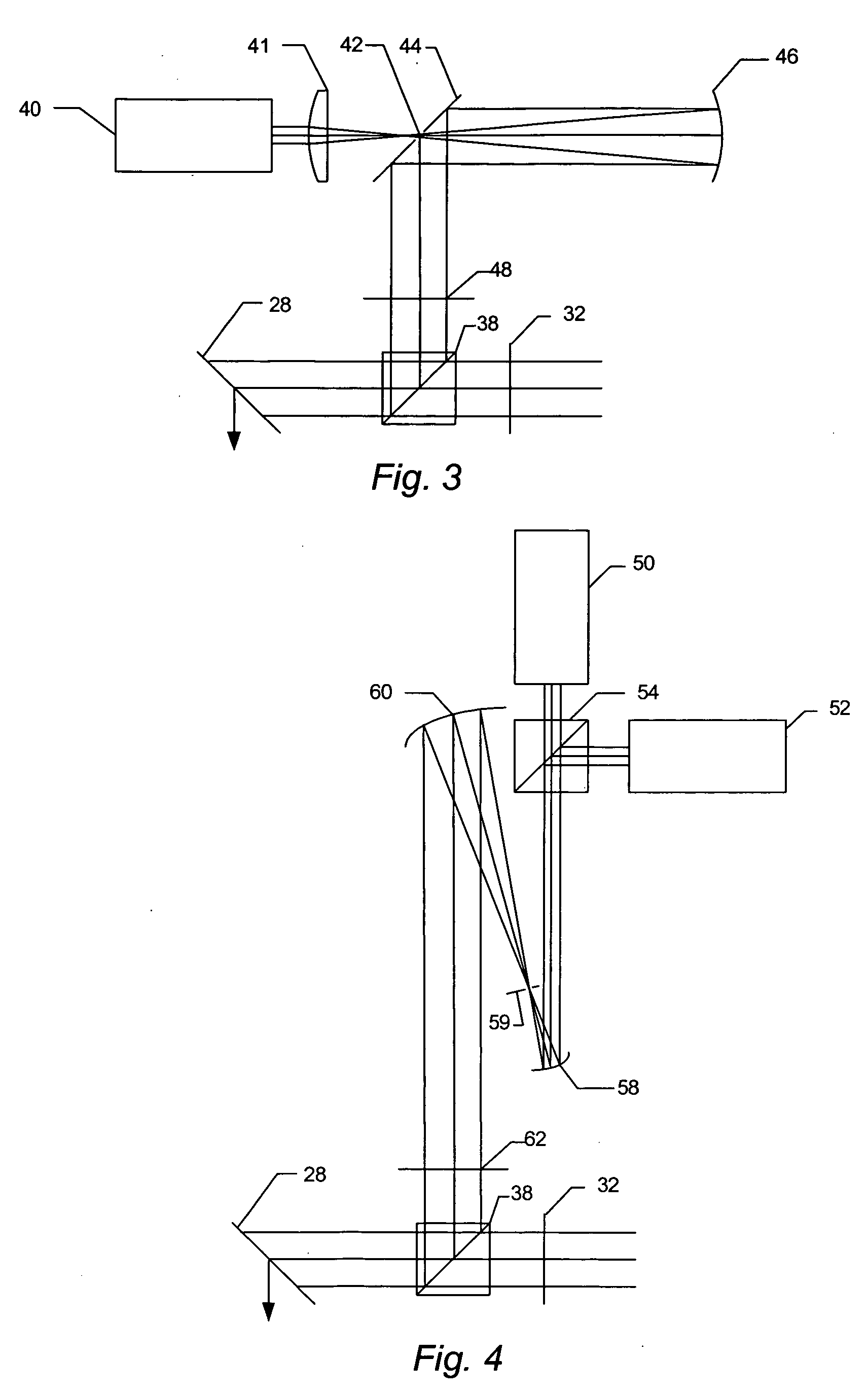
[0016] In one embodiment, the optical subsystem includes one or more light sources. In one embodiment, the one or more light sources include one or more fiber lasers. In another embodiment, the one or more light sources include a laser configure to generate light at multiple harmonics. In one such embodiment, the optical subsystem is configured to direct light at one of the multiple harmonics to the wafer, light at a plurality of the multiple harmonics to the wafer sequentially, or light at a plurality of the multiple harmonics to the wafer simultaneously. In a different embodiment, the one or more light sources include a cascade arc. In other embodiments, the one or more light sources include an arc lamp, a laser, a laser configured to generate light at multiple harmonics, or some combination thereof.
[0017] In another embodiment, the reflective optical components include two or more optical components that are configured to alter a magnification of light collected by the optical subsystem. In some embodiments, the optical subsystem is configured to have a magnification from about 50× to about 500×.
[0018] In an embodiment, the optical subsystem is configured to have a low central obscuration. In an additional embodiment, the optical subsystem is configured to have an accessible pupil separated in illumination and collection paths by a beamsplitter. In another embodiment, the optical subsystem is configured to have an accessible Fourier plane.
[0019] In some embodiments, the one or more refractive optical components include a refractive beamsplit...

Problems solved by technology

However, as the dimensions of semiconductor devices decrease, inspection becomes even more important to the successful manufacture of acceptable semiconductor devices because smaller defects can cause the device to fail.
For instance, as the dimensions of semiconductor devices decrease, detection of defects of decreasing size has become necessary since even relatively small defects may cause unwanted aberrations in the semiconductor devices.
Furthermore, thin-film interference between transparent layers on a semiconductor wafer can create measurement noise because of variations in the thickness of the layers.
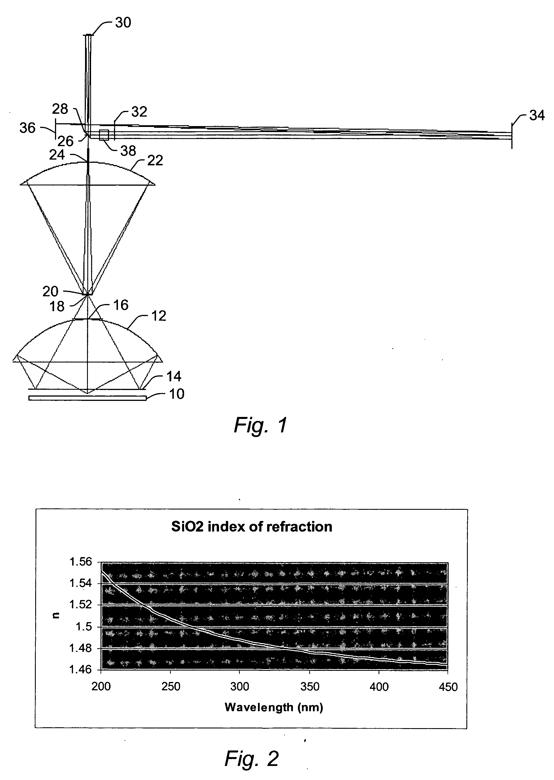
The material combinations described above, however, typically cannot be used for a broadband optical system designed to operate at wavelengths below 230 nm.
Therefore, the transmission properties of fused silica prohibit any broadband solution below that wavelength as there are not two dissimilar refractive materials available for use below that wavelength.
Therefore, although significant utility in wafer inspection applications has been found for these lenses, due to the transmission properties of fused silica described above, these lenses are not suited for broadband wafer inspection below wavelengths of 200 nm or even 230 nm.
These limitations are not specific to the lenses described in this patent but will be true for any inspection system that includes at least one lens element that is formed of fused silica.

Method used


Image

  • All-reflective optical systems for broadband wafer inspection
  • All-reflective optical systems for broadband wafer inspection
  • All-reflective optical systems for broadband wafer inspection

Examples


Embodiment Construction

[0031] As used herein, the term “defect” generally refers to any abnormality or undesirable feature that may be formed on or within a wafer.

[0032] As used herein, the term “wafer” generally refers to substrates formed of a semiconductor or non-semiconductor material. Examples of such a semiconductor or non-semiconductor material include, but are not limited to, monocrystalline silicon, gallium arsenide, and indium phosphide. Such substrates may be commonly found and / or processed in semiconductor fabrication facilities. A wafer may include one or more layers formed upon a substrate. For example, such layers may include, but are not limited to, a resist, a dielectric material, and a conductive material. Many different types of such layers are known in the art, and the term wafer as used herein is intended to encompass a wafer including all types of such layers.

[0033] One or more layers formed on a wafer may be patterned or unpatterned. For example, a wafer may include a plurality of...


PUM


Abstract

All-reflective optical systems for broadband wafer inspection are provided. One system configured to inspect a wafer includes an optical subsystem. All light-directing components of the optical subsystem are reflective optical components except for one or more refractive optical components, which are located only in substantially collimated space. The refractive optical component(s) may include, for example, a refractive beamsplitter element that can be used to separate illumination and collection pupils. The optical subsystem may also include one or more reflective optical components located in substantially collimated space. The optical subsystem is configured for inspection of the wafer across a waveband of greater than 20 nm. In some embodiments, the optical subsystem is configured for inspection of the wafer at wavelengths less than and greater than 200 nm.

Description

BACKGROUND OF THE INVENTION [0001] 1. Field of the Invention [0002] This invention generally relates to all-reflective optical systems for broadband wafer inspection. Certain embodiments relate to a system that includes an optical subsystem of which all light-directing optical components are reflective optical components except for one or more refractive optical components that are located in substantially collimated space such that the refractive optical component(s) do not introduce aberrations to the light. The reflective optical components are located in non-collimated space and substantially collimated space. [0003] 2. Description of the Related Art [0004] The following description and examples are not admitted to be prior art by virtue of their inclusion in this section. [0005] Fabricating semiconductor devices such as logic and memory devices typically includes processing a substrate such as a semiconductor wafer using a large number of semiconductor fabrication processes to ...

Claims


Application Information

Patent Timeline
IPC IPC(8): G01N21/88
CPCG01N21/9501G02B17/061G01N2201/0636G01N2021/9563
Inventor LANGE, STEVEN R.
Owner KLA TENCOR TECH CORP
Learn More