Resin composition for mold used in forming micropattern, and method for fabricating organic mold therefrom
- Summary
- Abstract
- Description
- Claims
- Application Information
AI Technical Summary
Benefits of technology
Problems solved by technology
Method used
Image
Examples
example 1-1
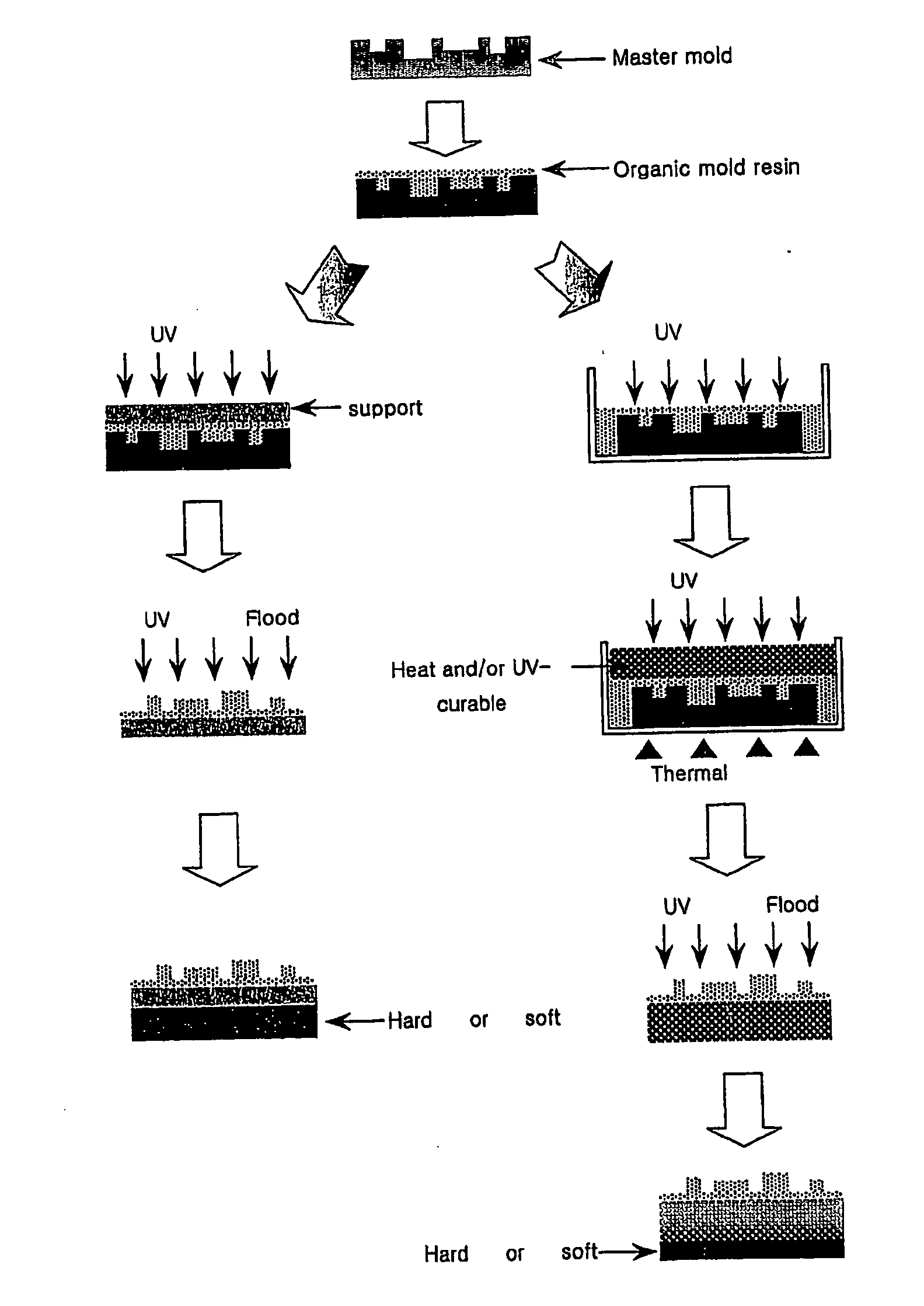
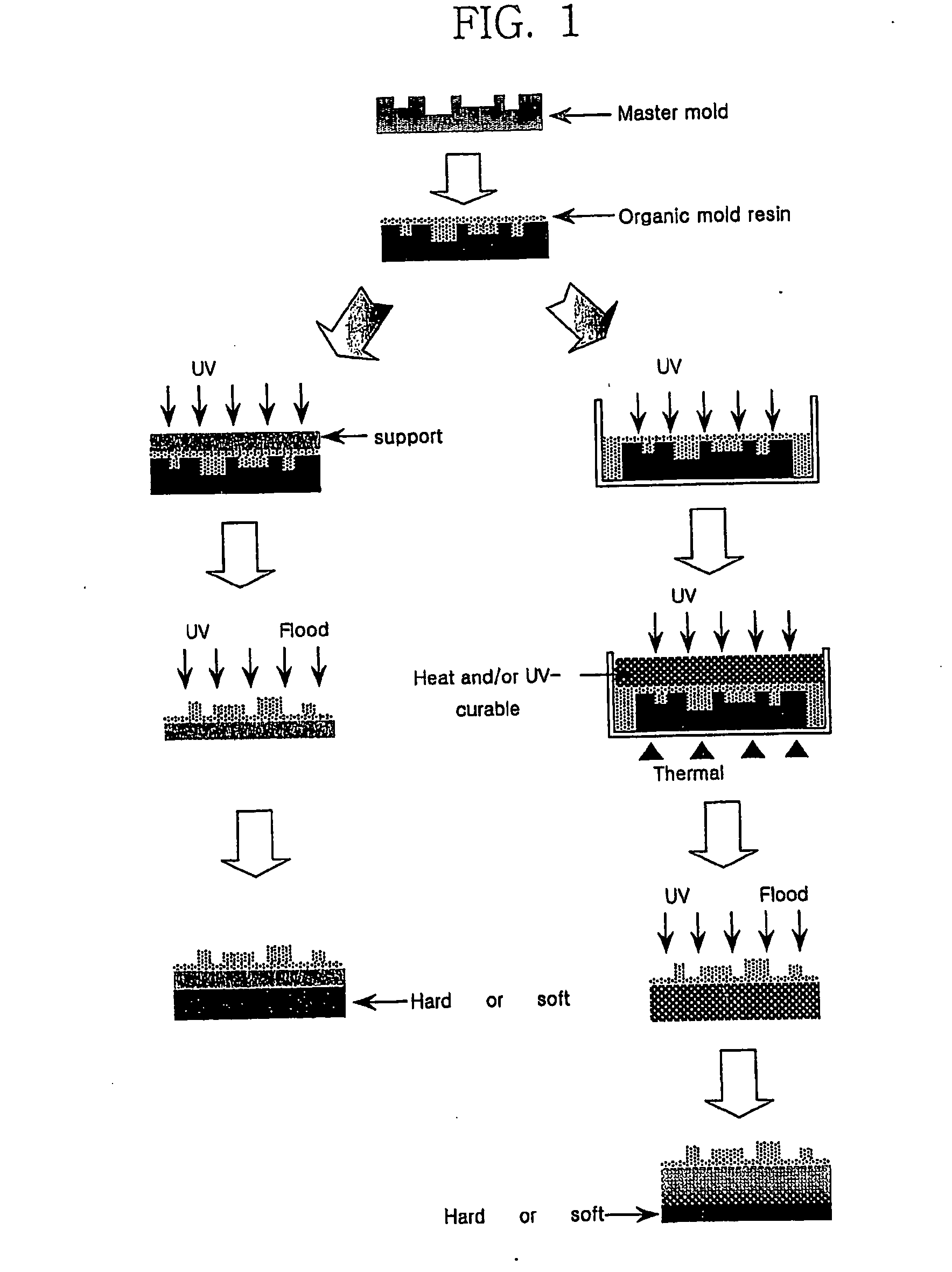
[0043] An organic mold was fabricated by a replicating method as shown in the procedure (a) of FIG. 1.
[0044] Specifically, a silicon mastermold having the reverse pattern structure of a desired resin pattern was prepared. A resin composition according to Preparation 1 was coated on the pattern face of the mastermold to a thickness of 15 μm. Then, a transparent adhesive polyethylene terephthalate sheet having a thickness of 188 μm was laid on the coated surface, and the resulting laminate was irradiated with a UV light of 5 mJ / cm2 for 15 seconds to cure the resin composition.
[0045] The cured organic mold was lifted off from the mastermold to obtain an organic mold having the desired pattern combined with a polyethylene terephthalate (PET) support. Then, UV (5 mJ / cm2) was additionally irradiated for 2 hours to completely cure the organic mold
example 1-2
[0046] A replicated organic mold was fabricated as shown in the procedure (b) of FIG. 1.
[0047] Specifically, the pattern surface of the silicon mastermold used in Example 1-1 is firstly coated with the resin composition of Preparation 1 to a thickness of 15 μm and pre-cured for 3 minutes with a UV light of 5 mJ / cm2. The laminate was placed in a vessel, and a UV curable, acrylated butadiene resin composition was poured and cured to form a backbone layer to a thickness of 2 mm.
[0048] The cured product was removed from the vessel and an organic mold having the desired pattern with an acrylated butadiene backbone was lifted off from the mastermold, and then additionally irradiated with UV (5 mJ / cm2) for 2 hours to completely cure the organic mold.
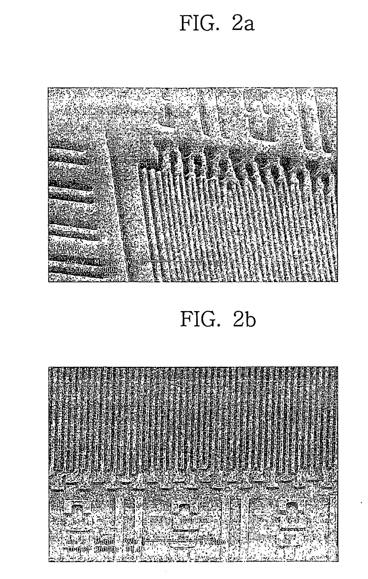
[0049]FIG. 2a is an electronic microscopic photograph of an organic mold fabricated as in Example 1-1 which has an equal line width and space of 80 nm.
[0050] Further, FIG. 3a is an electronic microscopic photograph of an organic mold having...
example 2-1
[0051] The organic mold shown in FIG. 2a was employed to form a pattern by a soft molding method. Specifically, a polystyrene resin solution was coated on a silicon wafer substrate and, on the coated resin layer, the mold was placed and slightly pressed to transfer the desired pattern on the polystyrene resin layer. FIG. 2b shows an electronic microscopic photograph of the pattern thus formed.
PUM
| Property | Measurement | Unit |
|---|---|---|
| Fraction | aaaaa | aaaaa |
| Percent by mass | aaaaa | aaaaa |
| Percent by mass | aaaaa | aaaaa |
Abstract
Description
Claims
Application Information
 - R&D
- Intellectual Property
- Life Sciences
- Materials
- Tech Scout
- Unparalleled Data Quality
- Higher Quality Content
- 60% Fewer Hallucinations
Browse by: Latest US Patents, China's latest patents, Technical Efficacy Thesaurus, Application Domain, Technology Topic, Popular Technical Reports.
© 2025 PatSnap. All rights reserved.Legal|Privacy policy|Modern Slavery Act Transparency Statement|Sitemap|About US| Contact US: help@patsnap.com


