
Integrated memory circuit and method for repairing a single bit error

a memory circuit and error repair technology, applied in the field of integrated memory circuits, can solve the problem of no longer being stored in the defective memory cell, and achieve the effect of improving yield

Inactive Publication Date: 2006-09-14
POLARIS INNOVATIONS
View PDF4 Cites 15 Cited by
  • Summary
  • Abstract
  • Description
  • Claims
  • Application Information

AI Technical Summary

Benefits of technology

[0006] It is an object of the present invention to provide an integrated memory circuit which enables a better yield in the case of assembly to form a memory module. It is furthermore an object of the present invention to provide a method which makes it possible to repair single bit errors in an integrated memory circuit after assembly to form a memory module.
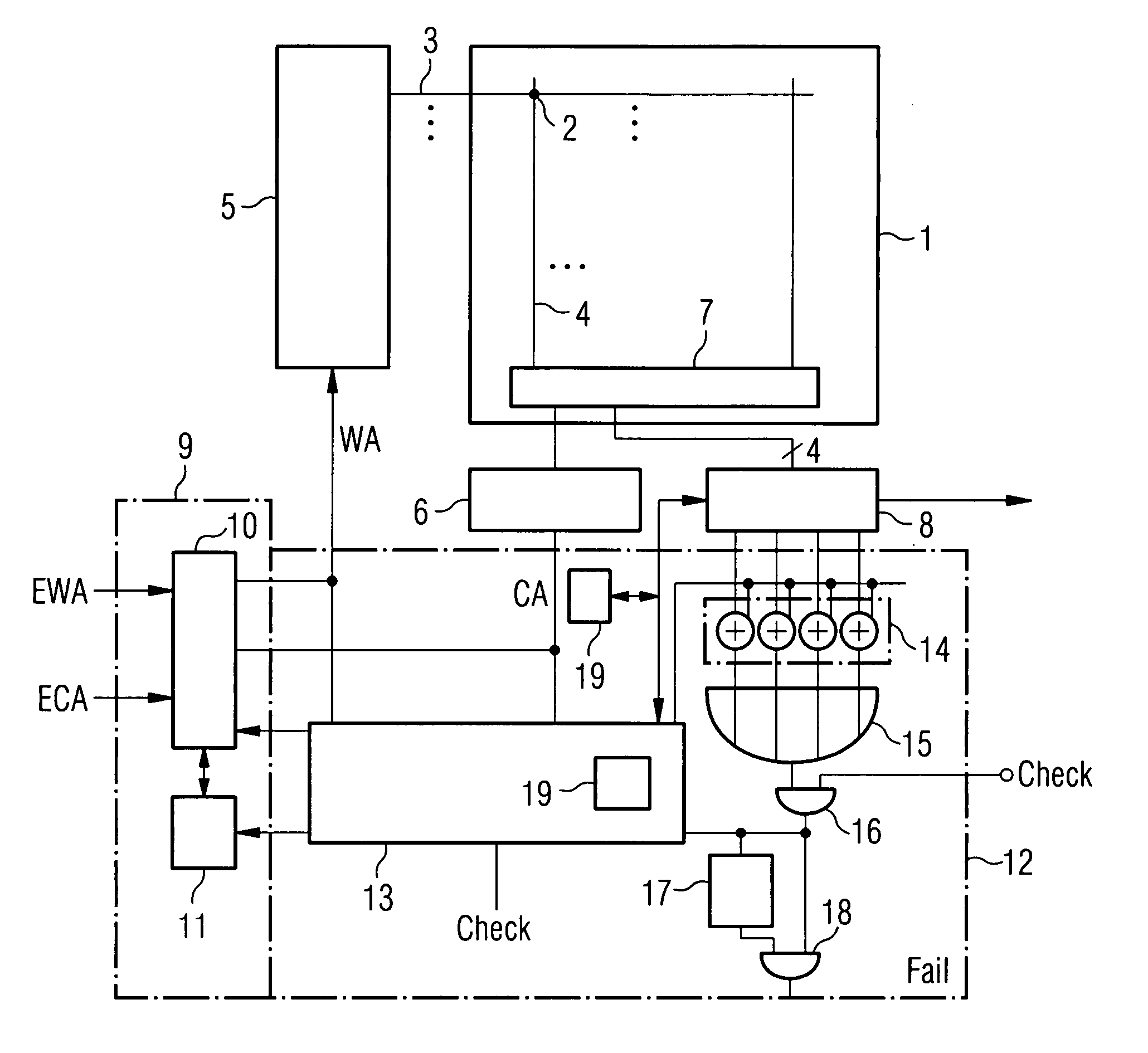
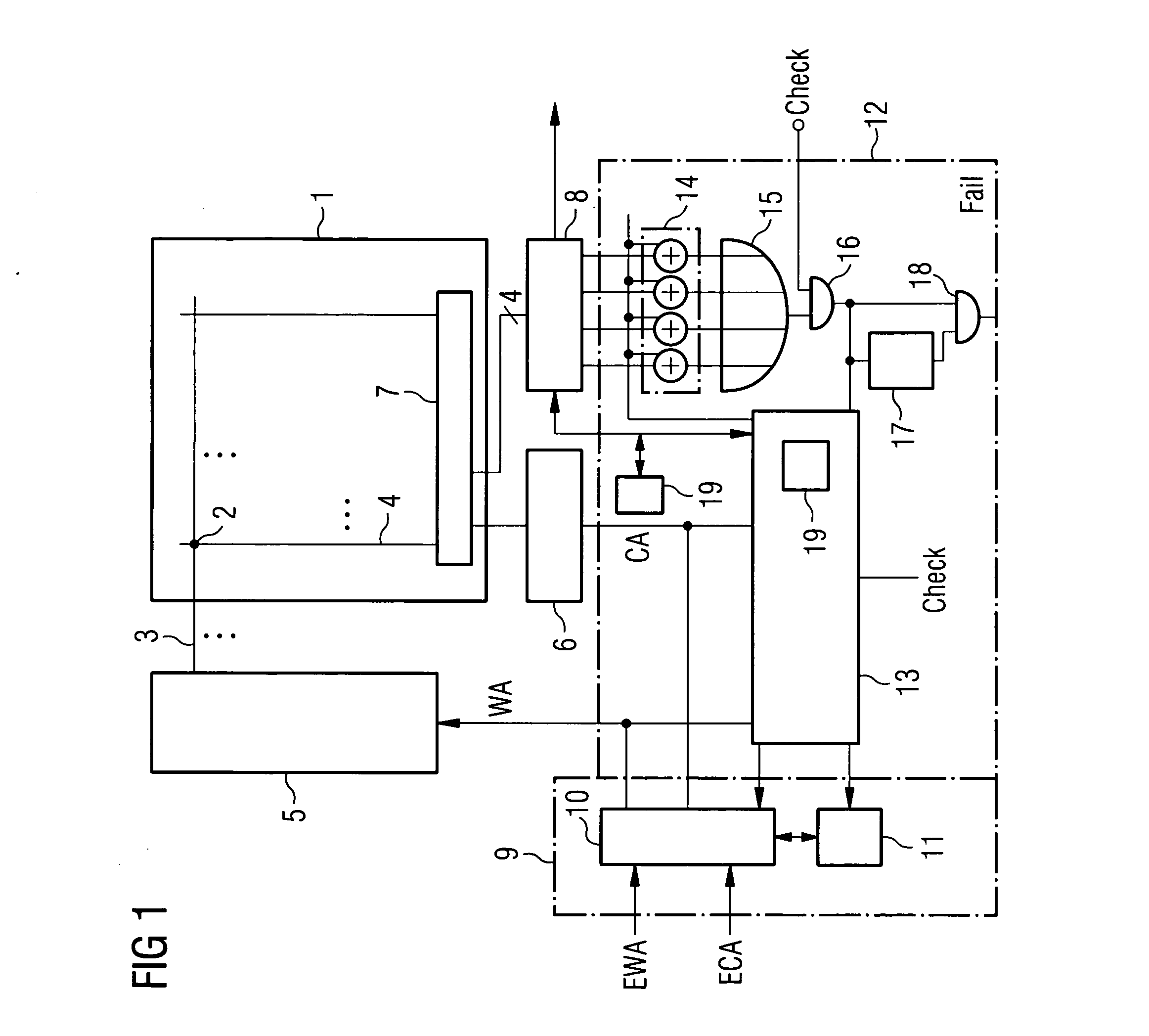
[0009] In order that an error in the case of which neither a logic “0” nor a logic “1” can be stored in the defective memory cell does not have the effect that the detected errors cancel one another out, the data read out after the writing of the first test data are modified in such a way that the position of each bit of the read-out data changes before the latter are written as second test data (in inverted fashion) to the memory area again. Since generally only single bit errors are to be expected anyway in the course of testing at the module level in the memory circuit to be tested (the probability of a plurality of memory cells failing is very low), it is possible, by comparing the data read out after the writing of the second test data with the expected data, to ascertain whether at least one error has occurred in the tested memory area. Since the repair circuit is provided in such a way that the entire memory area is replaced by a redundancy memory area as soon as an error has been detected, it is not necessary to determine the precise position of the single bit error in the memory area. The memory circuit according to the invention thus makes it possible, by the provision of a test unit configured in a simple manner, to determine an item of repair information by means of which, with the aid of the repair circuit, it is possible to repair a single bit error in the integrated memory circuit.
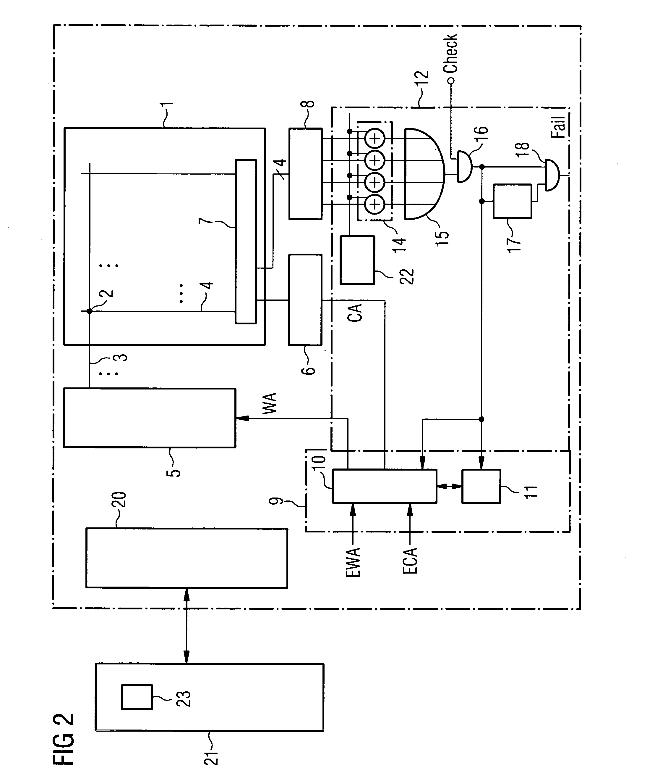
[0013] The integrated memory circuit in accordance with this aspect of the present invention has the advantage that the circuitry outlay for repairing the memory circuit is very low since only the repair on the basis of the repair information is performed within the integrated memory circuit, but not the provision of the test data, e.g. by means of a so-called BIST circuit. For this purpose, an interface unit is provided which is connected to an external test data unit, so that the testing of the memory cell array is performed by the external tester unit. The external tester unit makes the first and second test data available in such a way that the data stored after the writing of the second test data in the memory cell array correspond to the expected data provided by the expected data provision unit. In the case where the data stored in a memory area in the memory cell array deviate from the expected data, an error is detected, which leads to the generation of the repair information, as a result of which the relevant memory area is replaced by a redundant memory area.
[0016] The method according to the invention represents a simple possibility for automatically detecting a single bit error in a memory area of an integrated memory circuit and making available an item of repair information in this regard. The repair information serves for replacing the memory area having the defective memory cell by a redundancy memory area by programming of an error memory.

Problems solved by technology

Such a single bit error is usually manifested in the fact that after a thermal stress, either a logic “1” or a logic “0” can no longer be stored in the defective memory cell.

Method used


Image

  • Integrated memory circuit and method for repairing a single bit error
  • Integrated memory circuit and method for repairing a single bit error
  • Integrated memory circuit and method for repairing a single bit error

Examples


Embodiment Construction

[0022]FIG. 1 shows a block diagram of an integrated memory circuit in accordance with one preferred embodiment of the invention. The memory circuit comprises a memory cell array 1 having memory cells 2 which are arranged on word lines 3 and bit lines 4. The word lines 3 and the bit lines 4 form a matrix in which each memory cell 2 can be addressed by one of the word lines 3 and one of the bit lines 4. In the exemplary embodiment illustrated, the memory cells are preferably DRAM memory cells. However, it is also possible to provide any other memory cells which can be addressed via word lines 3 and bit lines 4. The word lines 3 are connected to a word line decoder 5, which, depending on a word line address WA, selects one of the word lines and activates the relevant word line 3 for accessing the addressed memory cell. With the aid of a column address CA, which is fed to a bit line decoder 6, the addressed bit lines are connected via a first sense amplifier 7 to a second sense amplifie...


PUM


Abstract

The invention relates to an integrated memory circuit having a memory cell array comprising memory cells arranged on word lines and bit lines, and having a repair circuit for repairing a single bit error in one of the memory cells, the repair circuit comprising: an error memory for storing an item of repair information, an assignment unit in order, when accessing an address of the memory cell array, depending on the repair information, to access either a memory area of the memory cell array or a redundancy memory area, and a test unit for determining the repair information. The test unit comprises a write unit, which successively writes first test data and second test data to a plurality of memory cells of a memory area of the memory cell array, a read-out unit which reads out data stored in the memory area, a modification unit in order to modify the bits of the read-out data in such a way that the position of each bit changes and each of the bits is inverted in order to provide the second test data, which are subsequently written to the memory area with the aid of the write unit, and a comparator unit in order to compare the data read out after the writing of the second test data with expected data and to provide the repair information depending on the comparison result.

Description

CROSS-REFERENCE TO RELATED APPLICATIONS [0001] This application claims foreign priority benefits under 35 U.S.C. §119 to co-pending German patent application number DE 10 2005 001 520.4, filed 13 Jan. 2005. This related patent application is herein incorporated by reference in its entirety. BACKGROUND OF THE INVENTION [0002] 1. Field of the Invention [0003] The invention relates to an integrated memory circuit having a memory cell array and a repair circuit for repairing a single bit error. The invention furthermore relates to a method for repairing a single bit error in an integrated memory circuit. [0004] 2. Description of the Related Art [0005] Memory cells of integrated memory circuits, in particular of DRAM memory circuits, may be subject to degradation if they are exposed to method steps with high temperatures, such as may occur for example during packaging or soldering. It can happen, therefore, that in the case of previously tested and error-free memory circuits, after assem...

Claims


Application Information

Patent Timeline
IPC IPC(8): G11C7/10
CPCG11C29/44G11C29/4401G11C2029/0405
Inventor POECHMUELLER, PETER
Owner POLARIS INNOVATIONS
Learn More