Optoelectronic package with wire-protection lid
a technology of optoelectronic packages and lids, which is applied in the direction of electrical apparatus casings/cabinets/drawers, semiconductor/solid-state device details, coupling device connections, etc., can solve the problems of easy short circuit to bonding wires, increased risk of light refraction, scattering, and wire collapse, and achieves the effect of improving the quality of the optoelectronic packag
- Summary
- Abstract
- Description
- Claims
- Application Information
AI Technical Summary
Benefits of technology
Problems solved by technology
Method used
Image
Examples
first embodiment
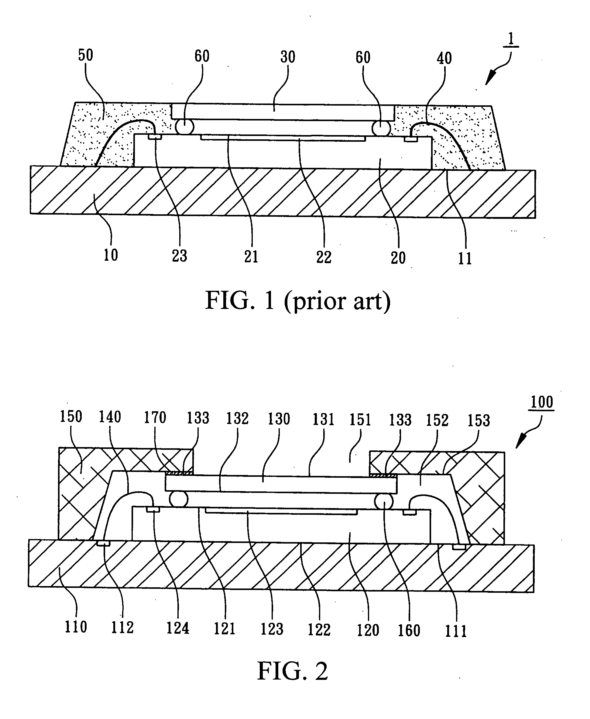
[0020] In the present invention, FIG. 2 is a schematic cross-sectional view of an optoelectronic package 100 with a wire-protection lid, and FIG. 3 is a top view of the optoelectronic package 100. Referring to FIG. 2, the optoelectronic package 100 mainly includes a substrate 110, a silicon die 120, a glass 130, a plurality of bonding wires 140, and a silicon base lid 150, wherein the substrate 110 has a top surface 111 with a plurality of connecting pads 112 being formed thereon. The substrate 110 can be a ceramic circuit board or another chip carrier.
[0021] The silicon die 120 has an active surface 121 and a back surface 122, wherein the active surface 121 includes a light working area 123 formed with a plurality of optical elements (not shown), and a plurality of pads 124 is formed on the active surface 121, and is disposed on other areas outside the light working area 123, for example, the edge area of the active surface 121. In the present embodiment, the silicon die 120 is a m...
second embodiment
[0028] In the present invention, referring to FIG. 6, an optoelectronic package 200 with a wire-protection lid can be applied to various forms of optoelectronic products, which mainly includes a substrate 210, a silicon die 220, a glass 230, a plurality of bonding wires 240, and a silicon base lid 250. The substrate 210 has a top surface 211 with a plurality of connecting pads 212 being formed thereon.
[0029] The silicon die 220 has an active surface 221 and a back surface 222. The active surface 221 of the silicon die 220 includes a light working area 223, and a plurality of pads 224 is formed on the active surface 221. In the present embodiment, the silicon die 220 is an image sensor chip, and the light working area 223 is formed with a plurality of image sensor elements (not shown).
[0030] In the present embodiment, the glass 230 is adhered and connected to the active surface 221 of the silicon die 220 with a transparent adhesive 260. The silicon die 220 is disposed on the top sur...
PUM
 Abstract
Description
Claims
Application Information
 - R&D
- Intellectual Property
- Life Sciences
- Materials
- Tech Scout
- Unparalleled Data Quality
- Higher Quality Content
- 60% Fewer Hallucinations
Browse by: Latest US Patents, China's latest patents, Technical Efficacy Thesaurus, Application Domain, Technology Topic, Popular Technical Reports.
© 2025 PatSnap. All rights reserved.Legal|Privacy policy|Modern Slavery Act Transparency Statement|Sitemap|About US| Contact US: help@patsnap.com


