Package structure with chip embedded in substrate

Inactive Publication Date: 2006-08-24
PHOENIX PRECISION TECH CORP
View PDF2 Cites 65 Cited by
  • Summary
  • Abstract
  • Description
  • Claims
  • Application Information

AI Technical Summary

Benefits of technology

[0008] In light of the foregoing drawbacks in the conventional technology, an objective of the present invention is to provide a package structure with chip embedded in substrate, which can effectively position a semiconductor chip in a chip carrier.
[0009] Another objective of the present invention is to provide a package structure with chip embedded in substrate, in which a plurality of semiconductor chips can be integrated to thereby improve the electrical performances of an electronic product incorporating the package structure.
[0010] Still another objective of the present invention is to provide a package structure with chip embedded in substrate, in which planarity and consistency of semiconductor elements embedded in a cavity of a carrier can be maintained to thereby improve capability of performing subsequent fine-circuit fabrication processes.

Problems solved by technology

Although such arrangement achieves incorporation of a large number of I / O connections in the semiconductor package structure, the electrical performances thereof are limited and hardly improved due to a long electrical connection path of wires during high-frequency or high-speed operation.
Moreover, since a plurality of connection interfaces are required for the conventional packaging processes, the fabrication costs are accordingly increased.
However, when the dielectric material flows into the recess 104, the space in the recess 104 cannot be completely filled with the dielectric material due to restriction of size of the recess 104 and surface tension of the dielectric material itself, thereby easy to cause gaps or voids.
During a subsequent thermal cycle for the semiconductor package, air within the gaps or voids may expand by heat to press the chip in the semiconductor package or even explode to damage the chip.
Moreover, since the dielectric material cannot fill the recess 104 completely, this results in poor surface planarity of the dielectric material, making the semiconductor package not able to be applied to high-level integrated circuit products.
Furthermore, although circuits can be directly extended from the chip in the foregoing semiconductor package to shorten the electrical connection path and improve the performance in high-speed operation, such semiconductor package is normally embedded with only one semiconductor chip and not able to provide a multi-functional module structure, such that the conventional packaging technology does not satisfy the development tendency of electronic products with the requirement of multi-functionality nowadays.

Method used


Image

  • Package structure with chip embedded in substrate
  • Package structure with chip embedded in substrate
  • Package structure with chip embedded in substrate

Examples


Embodiment Construction

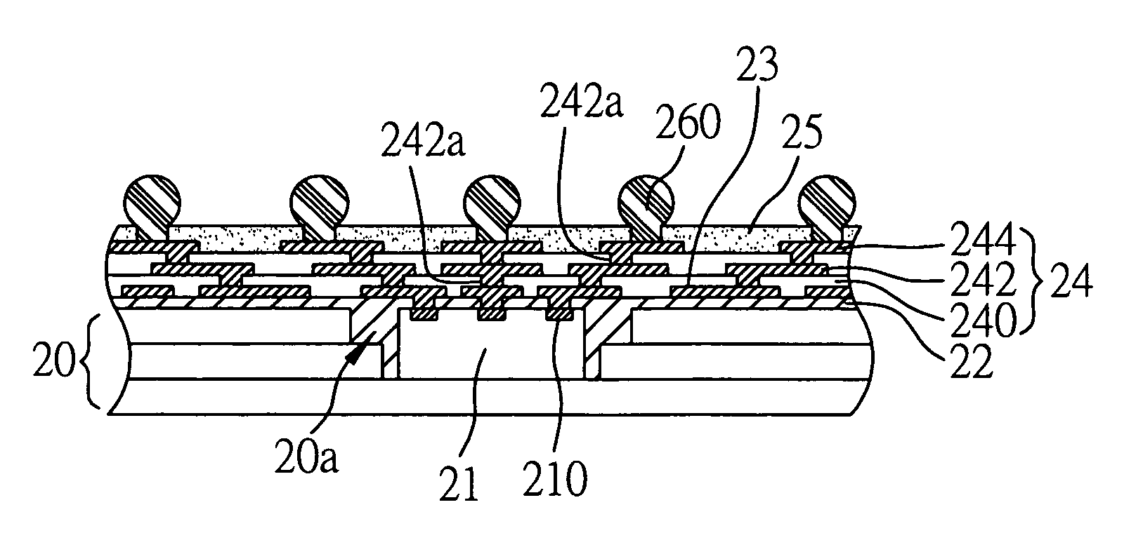
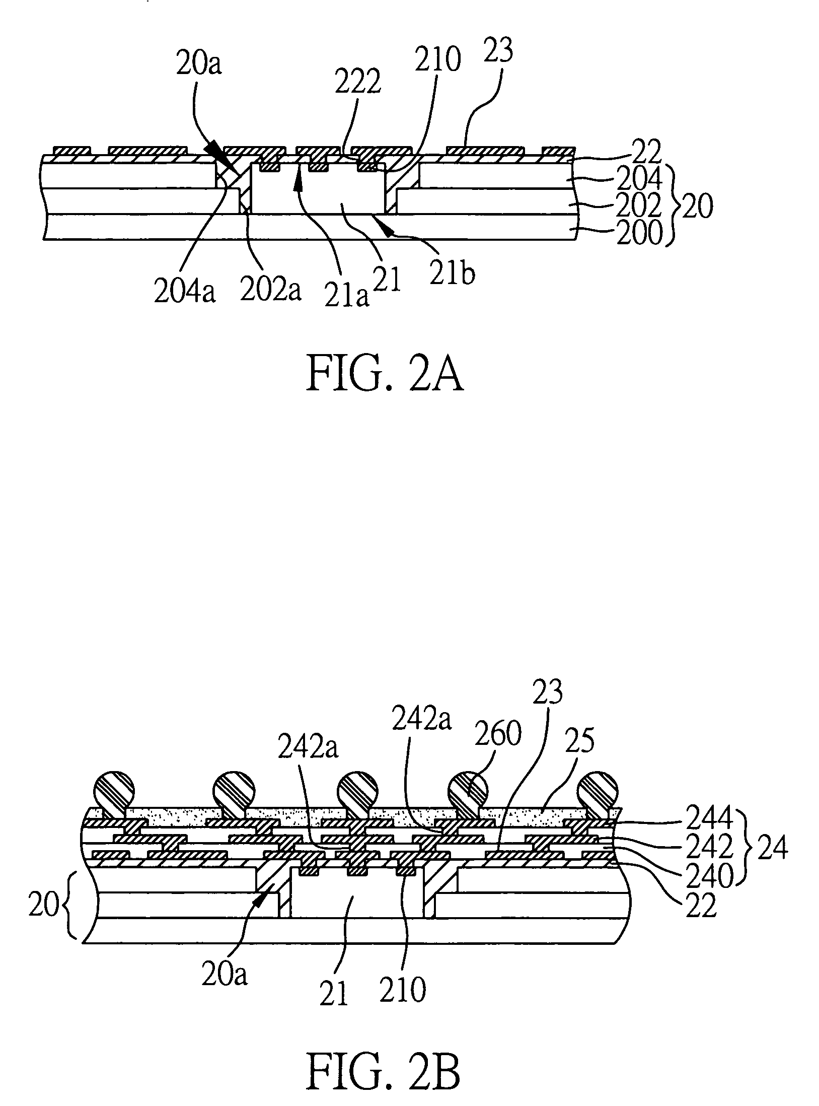
[0021]FIG. 2A shows a cross-sectional view of a package structure with chip embedded in substrate according to a first preferred embodiment of the present invention. As shown in FIG. 2A, the package structure comprises a carrier 20 having at least one stepped cavity 20a; at least one semiconductor chip 21 received in the stepped cavity 20a of the carrier 20; and a dielectric layer 22 formed on the semiconductor chip 21 and the carrier 20 and filled in a gap between the semiconductor chip 21 and the cavity 20a of the carrier 20 to fix the semiconductor chip 21 in the carrier 20. The package structure may further comprises a circuit layer 23 formed on the dielectric layer 22 and electrically connected to the semiconductor chip 21.

[0022] In this embodiment of the present invention, the carrier 20 is formed by stacking a plurality of carrier layers, wherein the carrier layers except the bottommost one are each provided with at least one through opening, and the openings are increased i...


PUM


Abstract

A package structure with chip embedded in substrate includes: a carrier having a stepped cavity; a semiconductor chip (or a chip set) received in the cavity of the carrier; a dielectric layer formed on the semiconductor chip and the carrier and filled in a gap between the semiconductor chip and the cavity of the carrier to fix the semiconductor chip in the carrier; and a circuit layer formed on the dielectric layer, and electrically connected to electrode pads of the semiconductor chip via a plurality of conductive structures so as to provide external electrical extension for the semiconductor chip via the circuit layer.

Description

FIELD OF THE INVENTION [0001] The present invention relates to package structures with chips embedded in substrates, and more particularly, to a package structure integrated with a semiconductor chip. BACKGROUND OF THE INVENTION [0002] There have been developed various package types of semiconductor devices along with evolution of the semiconductor packaging technology. Basically in a semiconductor package structure, a semiconductor chip is mounted on and electrically connected to a package substrate or lead frame, and then an encapsulant is formed for encapsulating the semiconductor chip. Ball Grid Array (BGA) package employs one of advanced semiconductor packaging technologies, which is characterized in that a package substrate is utilized for mounting a semiconductor chip on a front surface thereof, and a plurality of array-arranged solder balls are implanted on a back surface of the package substrate by using a self-alignment technique, thereby allowing more I / O connections (e.g...

Claims


Application Information

Patent Timeline
IPC IPC(8): H01L23/12
CPCH01L23/13H01L2224/0401H01L24/19H01L24/24H01L2224/04105H01L2224/20H01L2224/24227H01L2224/73267H01L2924/01082H01L2924/1433H01L2924/15153H01L2924/15165H01L2924/1517H01L2924/15311H01L2924/19041H01L23/5389H01L2224/92244H01L2224/32225H01L2224/12105H01L2924/10253H01L2924/01033H01L2924/00H01L2924/14
Inventor HSU, SHIH-PING
Owner PHOENIX PRECISION TECH CORP
Why Eureka
Try Eureka