
Advanced low dielectric constant organosilicon plasma chemical vapor deposition films

a technology of organosilicon and dielectric constant, applied in chemical vapor deposition coating, semiconductor/solid-state device details, coatings, etc., can solve the problems of increasing signal delay in ulsi electronic devices, poor mechanical properties, low modulus, etc., to improve the mechanical and electrical properties of inventive sicoh dielectric films, reduce the crosslinking of si—h and si—ch2—si, and increase the bonding of si—o—si

Active Publication Date: 2006-08-17
SONY CORP +2
View PDF17 Cites 67 Cited by
  • Summary
  • Abstract
  • Description
  • Claims
  • Application Information

AI Technical Summary

Benefits of technology

[0010] The higher degree of crystalline bonding interaction is believed to provide the inventive SiCOH dielectric material with improved mechanical strength as compared to prior art SiCOH dielectrics. Decreased amounts of methylene crosslinking groups present in the inventive film provides the film with a higher degree of porosity and increased polarization groups as compared to their prior art SiCOH counterparts.
[0012] The values mentioned above are for as deposited SiCOH dielectrics; without any post treatment steps being preformed. Post treatment such as UV treatment has been found to reduce the Si—H and Si—CH2—Si crosslinking bonding and increase the Si—O—Si bonding. The post treatment process can further improve the inventive SiCOH dielectric film's mechanical and electrical properties.

Problems solved by technology

This combined effect increases signal delays in ULSI electronic devices.
A key problem with prior art low and ultra low k SiCOH films is that they have poor mechanical properties (such as, for example, a high crack velocity and stress, and a low modulus and hardness).
Typically, the mechanical properties of prior art SiCOH dielectrics deteriorate as the dielectric constant of the material decreases.
Hence, porous SiCOH dielectrics tend to have poorer mechanical properties than the corresponding non-porous SiCOH dielectrics.
While such post deposition treatments are possible, they add extra processing steps and thus cost to the manufacturing of low k or ultra low k dielectric films.

Method used


Image

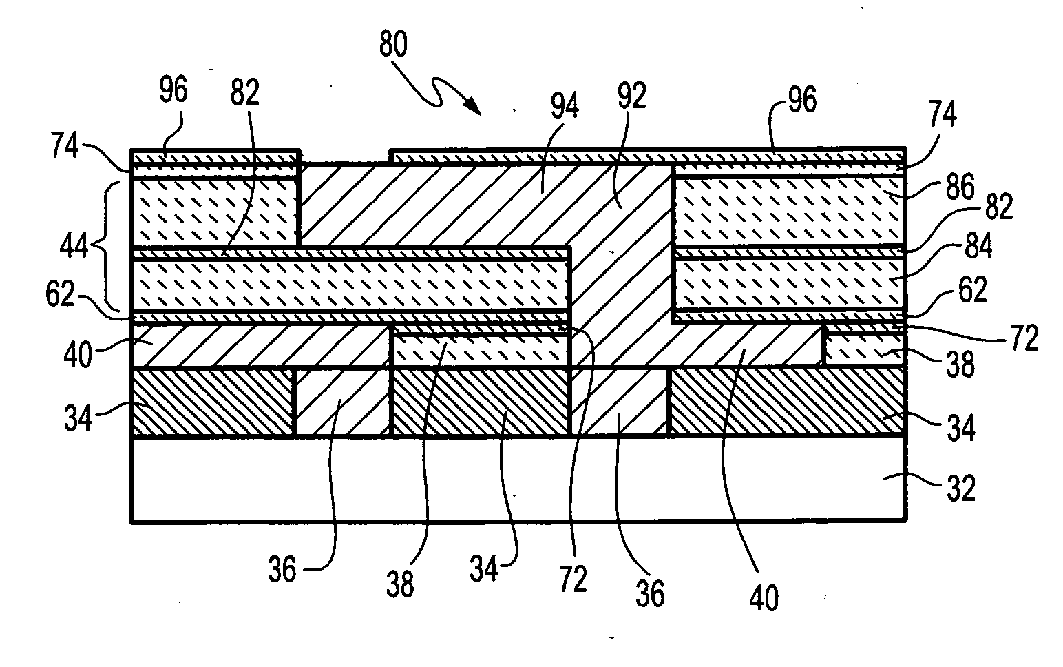
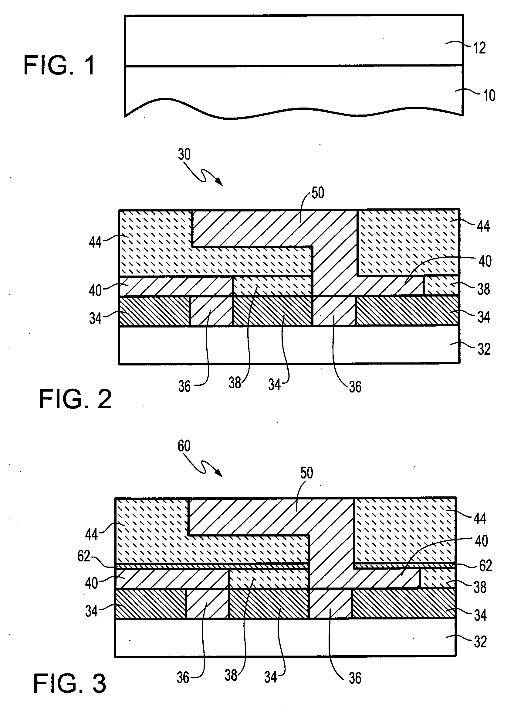
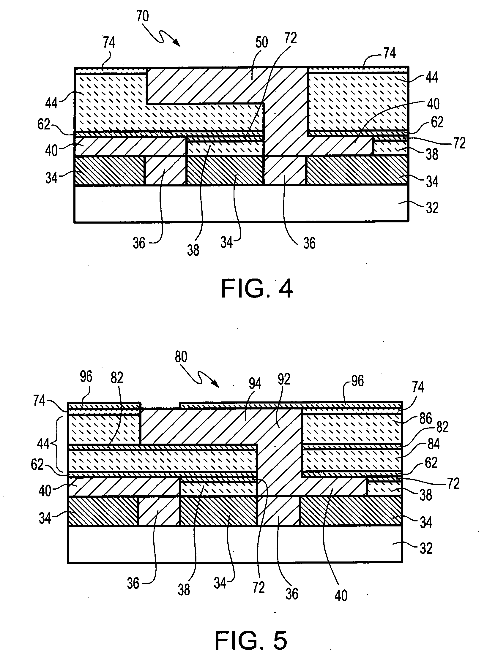
  • Advanced low dielectric constant organosilicon plasma chemical vapor deposition films
  • Advanced low dielectric constant organosilicon plasma chemical vapor deposition films
  • Advanced low dielectric constant organosilicon plasma chemical vapor deposition films

Examples


example

[0077] In this example, a SiCOH dielectric material of the present invention was prepared and it was compared with prior art SiCOH dielectrics. The inventive SiCOH dielectric (Sample A) was prepared using the method described above. The first precursor was OMCTS and the oxidizing agent was O2. The deposition conditions included: a OMCTS flow of 2800 mgm, an O2 flow of 220 sccm, a He carrier flow of 1000 sccm, a substrate deposition temperature of 350° C., a pressure of 5 Torr, a spacing of 450 mils, a HF power of 400 W, and a LF power of 60 W.

[0078] Another sample, Sample B, was made using the above procedure except that after deposition it was subjected to UV treatment.

[0079] Prior art SiCOH dielectric, Sample C was prepared using OMCTS as the precursor and the following conditions were used: a OMCTS flow of 2500 mgm, an O2 flow of 160 sccm, a He carrier flow of 1000 sccm, a substrate deposition temperature of 350° C., a pressure of 5 Torr, a spacing of 450 mils, a HF power of 50...


PUM

PropertyMeasurementUnit
porosityaaaaaaaaaa
dielectric constantaaaaaaaaaa

Abstract

A porous low k or ultra low k dielectric film comprising atoms of Si, C, O and H (hereinafter “SiCOH”) in a covalently bonded tri-dimensional network structure having a dielectric constant of less than about 3.0, a higher degree of crystalline bonding interactions, more carbon as methyl termination groups and fewer methylene, —CH2— crosslinking groups than prior art SiCOH dielectrics is provided. The SiCOH dielectric is characterized as having a FTIR spectrum comprising a peak area for CH3+CH2 stretching of less than about 1.40, a peak area for SiH stretching of less than about 0.20, a peak area for SiCH3 bonding of greater than about 2.0, and a peak area for Si—O—Si bonding of greater than about 60%, and a porosity of greater than about 20%.

Description

FIELD OF THE INVENTION [0001] The present invention relates to dielectric materials comprising atoms of Si, C, O and H (hereinafter “SiCOH” dielectric materials), which are porous and have a dielectric constant (k) on the order of less than about 3.0, and methods for fabricating films of these materials and electronic devices containing such films. The SiCOH dielectric material of the present invention has higher porosity, as compared with prior art SiCOH dielectric materials, and a higher degree of crystalline bonding interaction that leads to improved mechanical properties. The present invention also relates to a non-equilibrium method to fabricate the inventive material as well as to the use of said dielectric material as an intralevel or interlevel dielectric film, a dielectric cap or a hard mask / polish stop in back end of the line (BEOL) interconnect structures on ultra-large scale integrated (ULSI) circuits and related electronic structures. BACKGROUND OF THE INVENTION [0002] ...

Claims


Application Information

Patent Timeline
Patent Type & Authority Applications(United States)
IPC IPC(8): H01L21/31
CPCH01L21/02348H01L21/02351H01L21/02354H01L21/3122H01L21/31633H01L21/7682C23C16/401H01L21/02126H01L21/02203H01L21/02216H01L21/02274H01L21/0234H01L2221/1047H01L21/02211H01L21/31
Inventor NGUYEN, SONLANE, SARAH L.LEE, JIAIDA, KENSAKURESTAINO, DARRYL D.NOGAMI, TAKESHI
Owner SONY CORP
Learn More