
Semiconductor production system and semiconductor production process

a production system and semiconductor technology, applied in semiconductor/solid-state device testing/measurement, process and machine control, instruments, etc., can solve the problems of volume error ratio, treatment is more susceptible to flow volume error ratio, and actual flow volume deviating from the set flow volum

Active Publication Date: 2006-08-03
TOKYO ELECTRON LTD
View PDF9 Cites 13 Cited by
  • Summary
  • Abstract
  • Description
  • Claims
  • Application Information

AI Technical Summary

Benefits of technology

[0015] The present invention has been made in view of the foregoing disadvantages. One object of the present invention is to provide a semiconductor manufacturing apparatus and a semiconductor manufacturing method, in which a flow volume can be precisely set, without detaching a massflow controller from a pipe.
[0017] According to the present invention, in order to compensate a drift of the detected voltage when a flow volume is zero, the massflow controller is not adjusted, but a set voltage is corrected. As a result, a flow volume characteristic of the massflow controller can be exactly controlled in a simple manner.
[0021] According to the present invention, in order to compensate a change of a relationship between a set voltage and a flow volume, the massflow controller is not adjusted, but a set voltage is corrected. As a result, a flow volume characteristic of the massflow controller can be exactly controlled in a simple manner.
[0025] According to the present invention, in order to compensate a shift in a relationship between the set voltage and the flow volume, the massflow controller itself is not adjusted, but a set voltage is corrected. As a result, a flow volume characteristic of the massflow controller can be exactly controlled in a simple manner.

Problems solved by technology

However, while the massflow controller is used, it sometimes occurs that an actual flow volume deviates from the set flow volume.
For example, even if an actual flow volume is zero, there may be a case in which a voltage value outputted from the flow volume detecting unit is not zero, which is an error.
This may be caused by, for example, a difference between an environmental temperature at the time of shipment by a manufacturer and an environmental temperature on a user's side; deterioration with elapse of the time of a coating material of a coil-like heating resistance wire (sensor); separation of a coating material from a heating resistance wire; slack of a coil of a heating resistance wire; malfunction of a circuit part; variation of a power supply voltage; and pollution (caused by corrosion or adhesion of product) of a pipeline wrapped with a sensor.
As for a flow volume capable of being set in a massflow controller, a treatment is more susceptible to a flow volume error ratio of a smaller flow volume than a flow volume error ratio of a larger flow volume, under a condition of the same drift amount.
However, the use of a plurality of massflow controllers is disadvantageous in terms of costs.
In addition, when an output is drifted, that is, when a fluid flow volume is zero but an output voltage therefor is not zero, the drifted output may have an adverse effect on a treatment.
Since the method disclosed in Japanese Patent Laid-Open Publication No. 263350 / 1995 needs an additional measuring device, the method is disadvantageous in terms of costs.
Further, if the measuring device itself is broken, the massflow controller cannot be handled.
Thus, adjustment of the massflow controller at frequent intervals is troublesome.
However, when the massflow controller is replaced with a massflow controller of another manufacturer, the new massflow controller cannot be adjusted.
In addition, there is a need for a mechanism for supplying a current to a bridge circuit while gradually changing a value of the current, which disadvantageously complicates a constitution of an apparatus.

Method used


Image

  • Semiconductor production system and semiconductor production process
  • Semiconductor production system and semiconductor production process
  • Semiconductor production system and semiconductor production process

Examples


Embodiment Construction

[0041] Embodiments of the present invention are described below, with reference to the accompanying drawings.

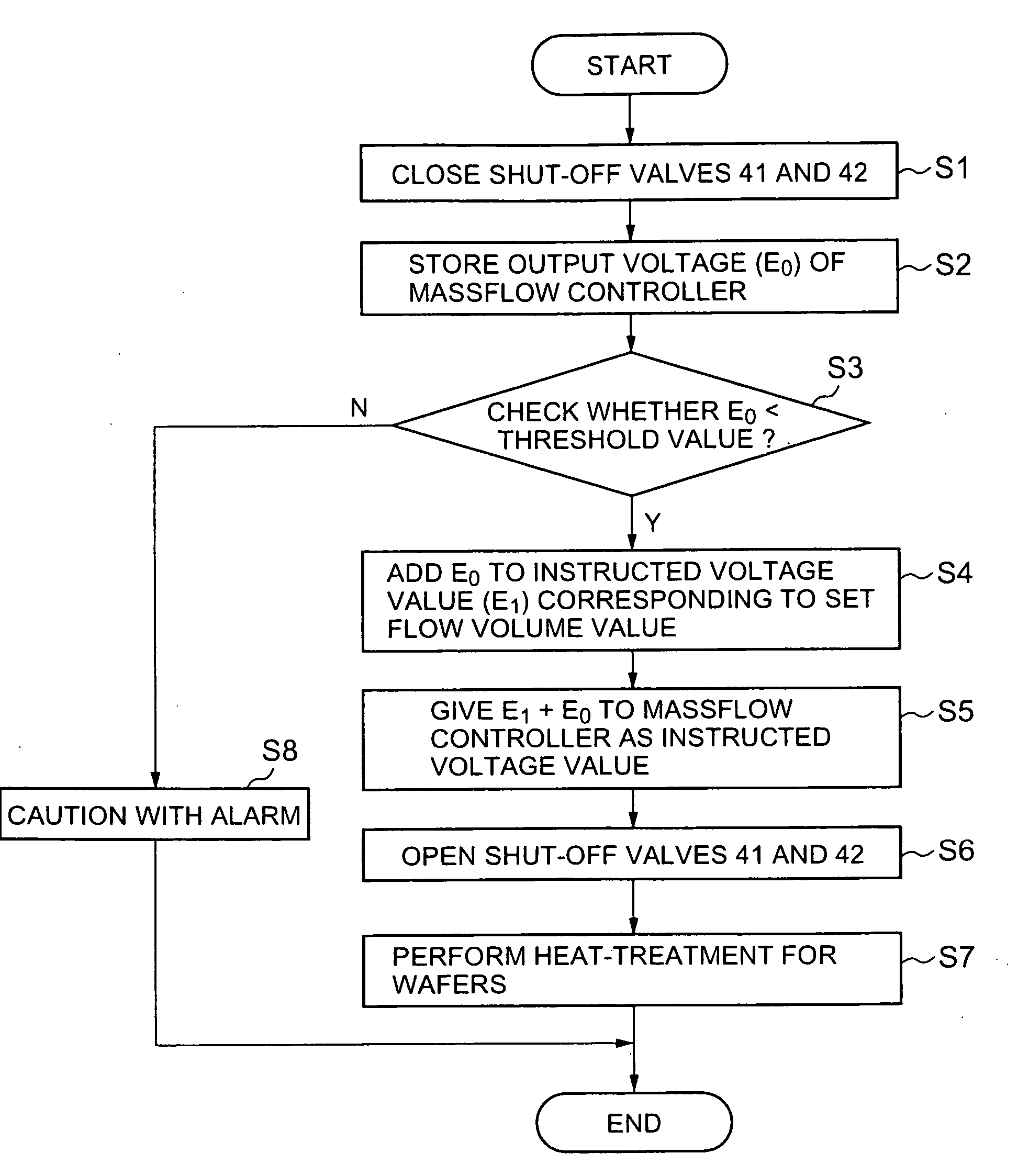
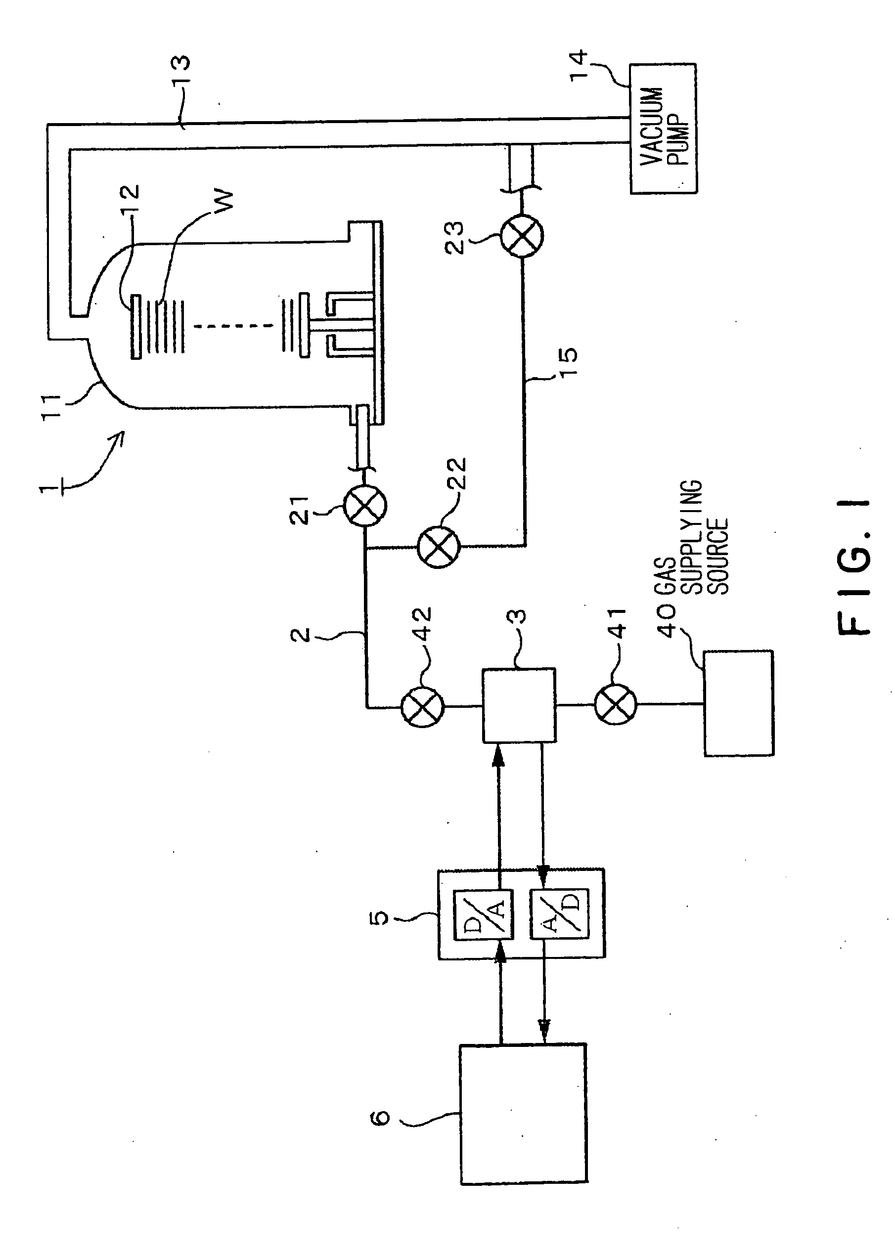
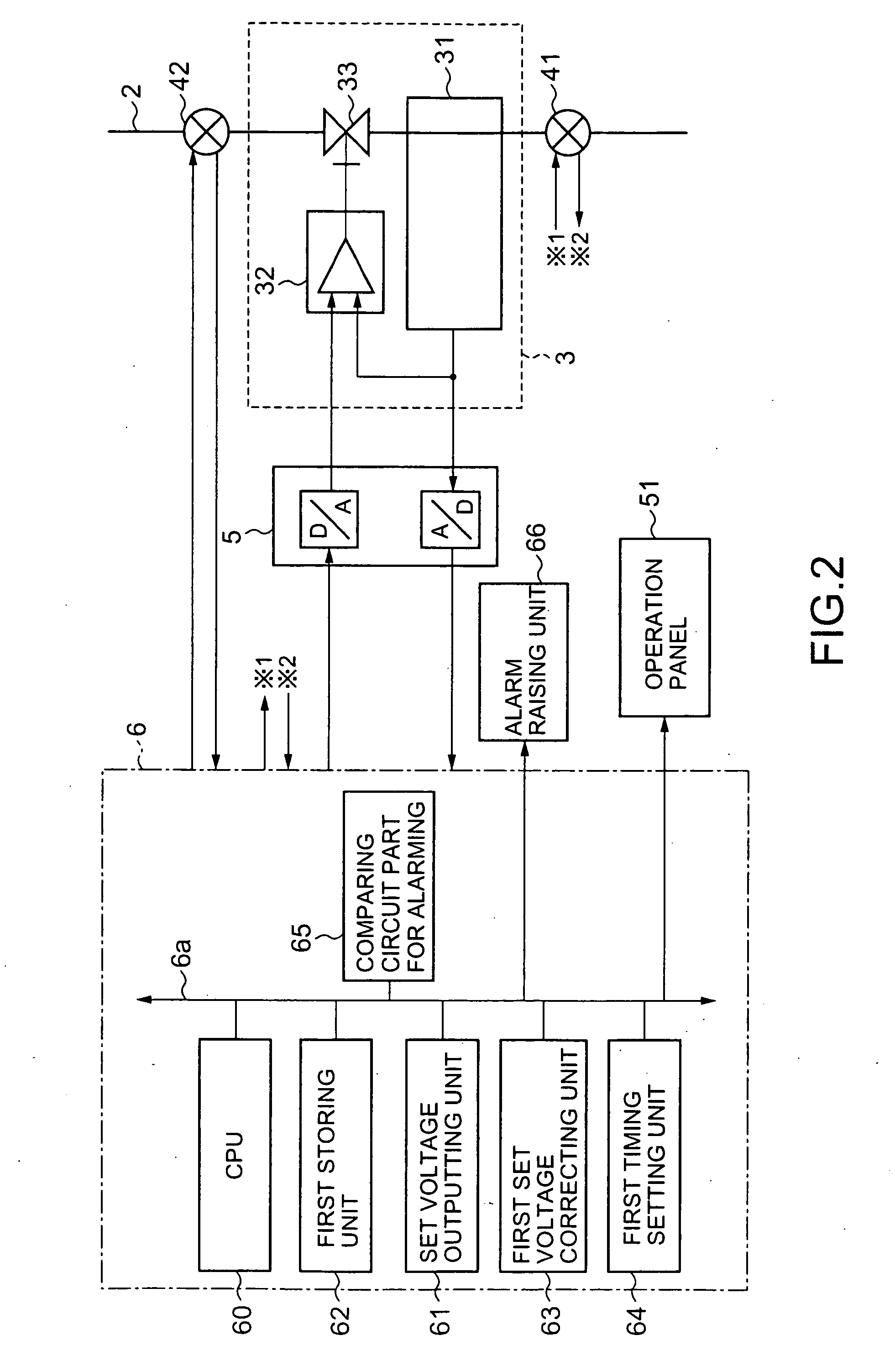
[0042]FIG. 1 is a block diagram schematically showing a structure of a semiconductor manufacturing apparatus in one embodiment according to the present invention. The semiconductor manufacturing apparatus includes a heat-treating unit 1 that performs a treatment for a substrate to manufacture thereon a semiconductor integrated circuit. A holder 12 holding a plurality of substrates such as wafers W is loaded into a vertical reaction tube 11 which is a reaction vessel (treatment vessel) of the heat-treating unit 1. The wafers W in the reaction tube 11 are heated by heating means, not shown, disposed outside the reaction tube 11. At the same time, a predetermined gas is introduced into the reaction tube 11 through a gas supplying channel 2 formed of, e.g., a gas supplying pipe. In this manner, a predetermined heat treatment is performed for the substrates. In FIG. 1, the refere...


PUM


Abstract

A semiconductor manufacturing apparatus according to the present invention comprises: a treating unit that treats a substrate to manufacture thereon a semiconductor device; a fluid supplying channel for supplying a fluid required for a treatment of the substrate to the treating unit; a set voltage outputting unit that outputs a set voltage corresponding to a set flow volume of the fluid; a massflow controller disposed on the fluid supplying channel, that controls a flow volume of the fluid based on the set voltage; a first shut-off valve disposed on the fluid supplying channel on an upstream side of the massflow controller; and a second shut-off valve disposed on the fluid supplying channel on a downstream side of the massflow controller. The massflow controller includes: a detecting unit that detects an actual flow volume of the fluid and outputs a corresponding detected voltage; a comparing unit that compares the set voltage with the detected voltage to output an operation signal; and a flow volume adjusting unit that adjusts the flow volume of the fluid based on the operation signal. A storing unit is provided, that stores the detected voltage outputted from the detecting unit of the massflow controller, when the first and the second shut-off valves are closed. A set voltage correcting unit is provided, that corrects the set voltage based on the detected voltage stored in the storing unit, in such a manner that a drift of the detected voltage is compensated when an actual flow volume of the fluid is zero.

Description

BACKGROUND OF THE INVENTION [0001] 1. Field of the Invention [0002] The present invention relates to a semiconductor manufacturing apparatus that performs a treatment for a substrate, such as a semiconductor wafer, with the use of a fluid of which flow volume is adjusted by a massflow controller. [0003] 2. Background Art [0004] A semiconductor manufacturing process conventionally includes a step in which a substrate is treated with a predetermined gas or liquid. As a treatment step with a gas, there are, for example, a film deposition step with a film deposition gas, an oxidation step with an oxidation gas, and an etching step with an etching gas. As a treatment step with a liquid, there are., for example, a step of supplying a resist liquid to a substrate, and a step of applying on a substrate a chemical liquid containing a precursor of an insulation film. [0005] Recently, in order to cope with a finer pattern of a semiconductor device, a thinner film thickness is required. Thus, a...

Claims


Application Information

Patent Timeline
Patent Type & Authority Applications(United States)
IPC IPC(8): H01L21/66H01L23/58G01R31/26G01F1/00G05D7/06H01L21/205H01L21/22
CPCG01F1/68G01F15/024G01F25/0007G05D7/0629G05D7/0635G01F25/10H01L21/67017H01L21/67253
Inventor OKABE, TSUNEYUKIKANEKO, KENGO
Owner TOKYO ELECTRON LTD
Learn More