Pixel circuit, display and driving method thereof

a technology of pixel circuit and drive method, applied in the field of pixel circuit, can solve the problems of small gate voltage drop and drain current suppression

Inactive Publication Date: 2006-08-03
SONY CORP
View PDF5 Cites 280 Cited by
  • Summary
  • Abstract
  • Description
  • Claims
  • Application Information

AI Technical Summary

Benefits of technology

[0014] According to the embodiments of the present invention, a pixel circuit includes a correction unit that corrects an input voltage (gate voltage) for a drive transistor before an emission period or at the beginning of the emission period, in order to cancel the dependence of the output current from the drive transistor on the carrier mobility. The correction unit operates during part of a sampling period, to extract the output current (drain current) from the drive transistor while the potential of a video signal (signal potential) is sampled, and negatively feed back the output current to a capacitive part, to thereby correct the input voltage (gate voltage). As is apparent from Equation 1, the output current (drain current) is proportional to the mobility. Therefore, when a drive transistor in a certain pixel has a high mobility, the output current from the drive transistor is correspondingly large. This output current is negatively fed back to the capacitive part to thereby correct the input voltage (gate voltage). A larger mobility results in a larger negative feedback amount, and therefore the input voltage (gate voltage) is greatly decreased correspondingly. This decrease of the gate voltage results in suppression of the drain current. In contrast, when a drive transistor in another pixel is relatively small, the drain current from the drive transistor is also small. Therefore, the amount of negative feedback to a capacitive part is also small, which leads to a small decrease of the gate voltage. That is, a smaller mobility of a drive transistor provides a smaller output current, which results in a smaller amount of correction. As described above, the correction unit according to the embodiments of the present invention corrects an input voltage by feedback so as to cancel variation in the mobility, and thus uniformity of a screen is improved. In addition, this mobility correction is carried out while a signal potential is sampled. The amplitude of a video signal potential changes corresponding to a gray-scale level range from a black level to a white level. At any level, the mobility correction can be implemented adequately. The amount of negative feedback to an input voltage depends on a time period for extracting an output current. A longer extraction time period offers a larger negative feedback amount. The embodiments of the present invention can vary the time period for extracting an output current within a sampling period, to thereby allow optimization of the negative feedback amount. Furthermore, in the embodiments of the invention, light-emitting elements are current-driven due to sampling of video signal potentials. The embodiments of the invention are the same as liquid crystal displays in the past in that the sampling of video signal potentials is implemented. Therefore, a voltage signal driver, which has been widely used in active-matrix liquid crystal displays in the past, can be used for a signal part in the embodiments of the invention. In addition, similarly to active-matrix liquid crystal panels in the past on which poly-silicon transistors are integrally formed, a display of one embodiment of the invention can also be fabricated as a peripheral-circuit-incorporated panel, in which peripheral scanner part and signal part are integrated with a pixel array part.

Problems solved by technology

This decrease of the gate voltage results in suppression of the drain current.
Therefore, the amount of negative feedback to a capacitive part is also small, which leads to a small decrease of the gate voltage.

Method used


Image

  • Pixel circuit, display and driving method thereof
  • Pixel circuit, display and driving method thereof
  • Pixel circuit, display and driving method thereof

Examples


Embodiment Construction

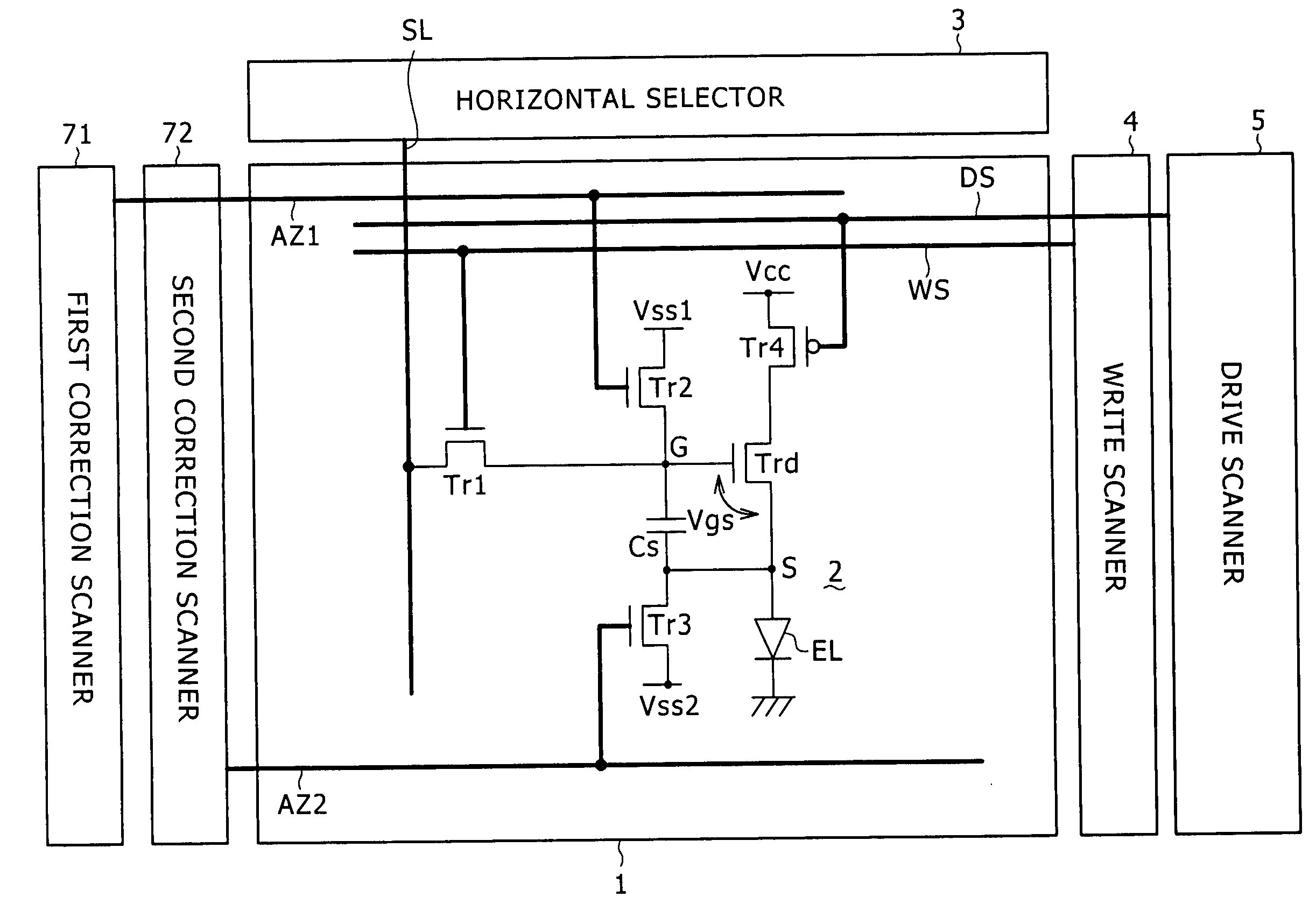
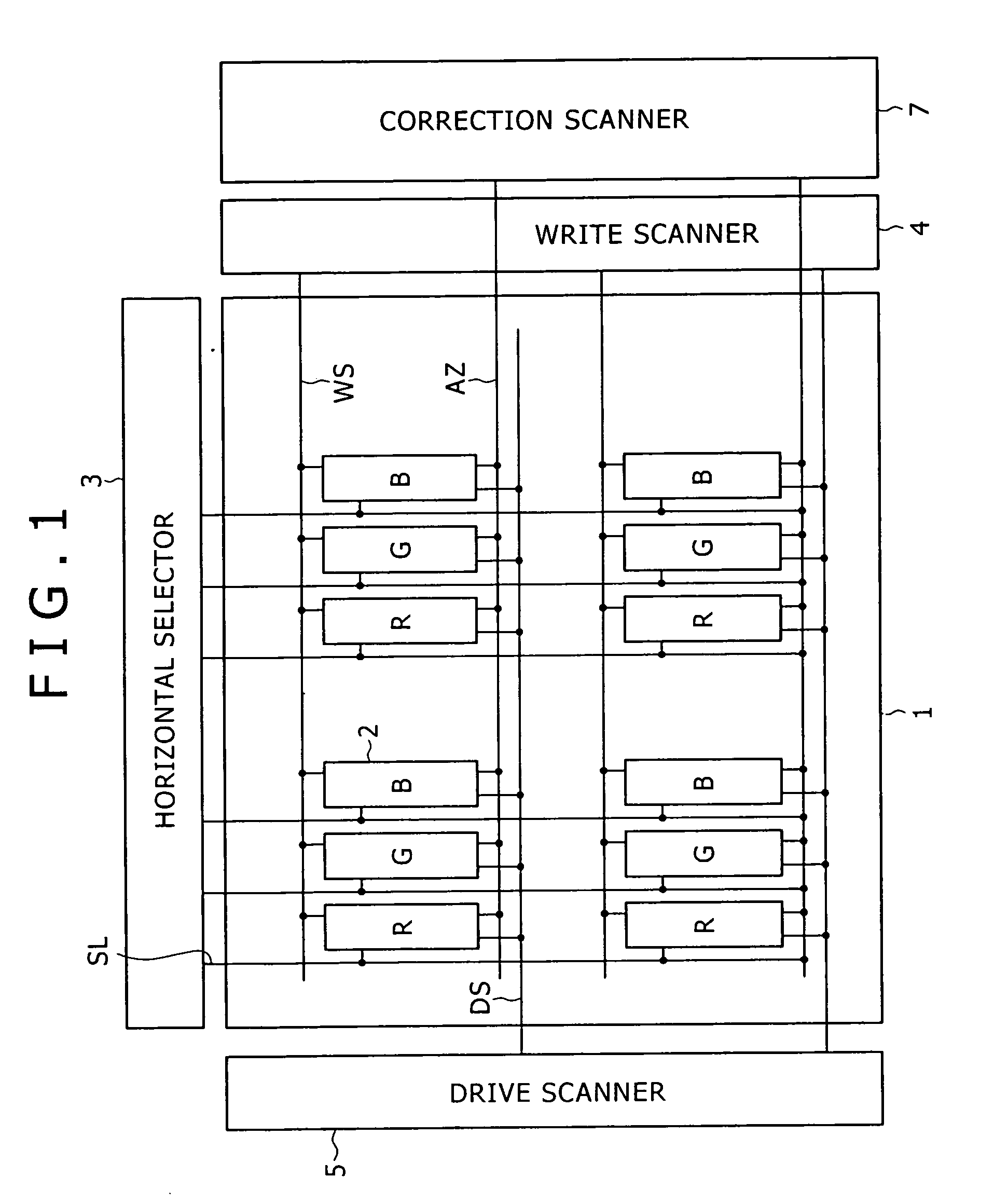
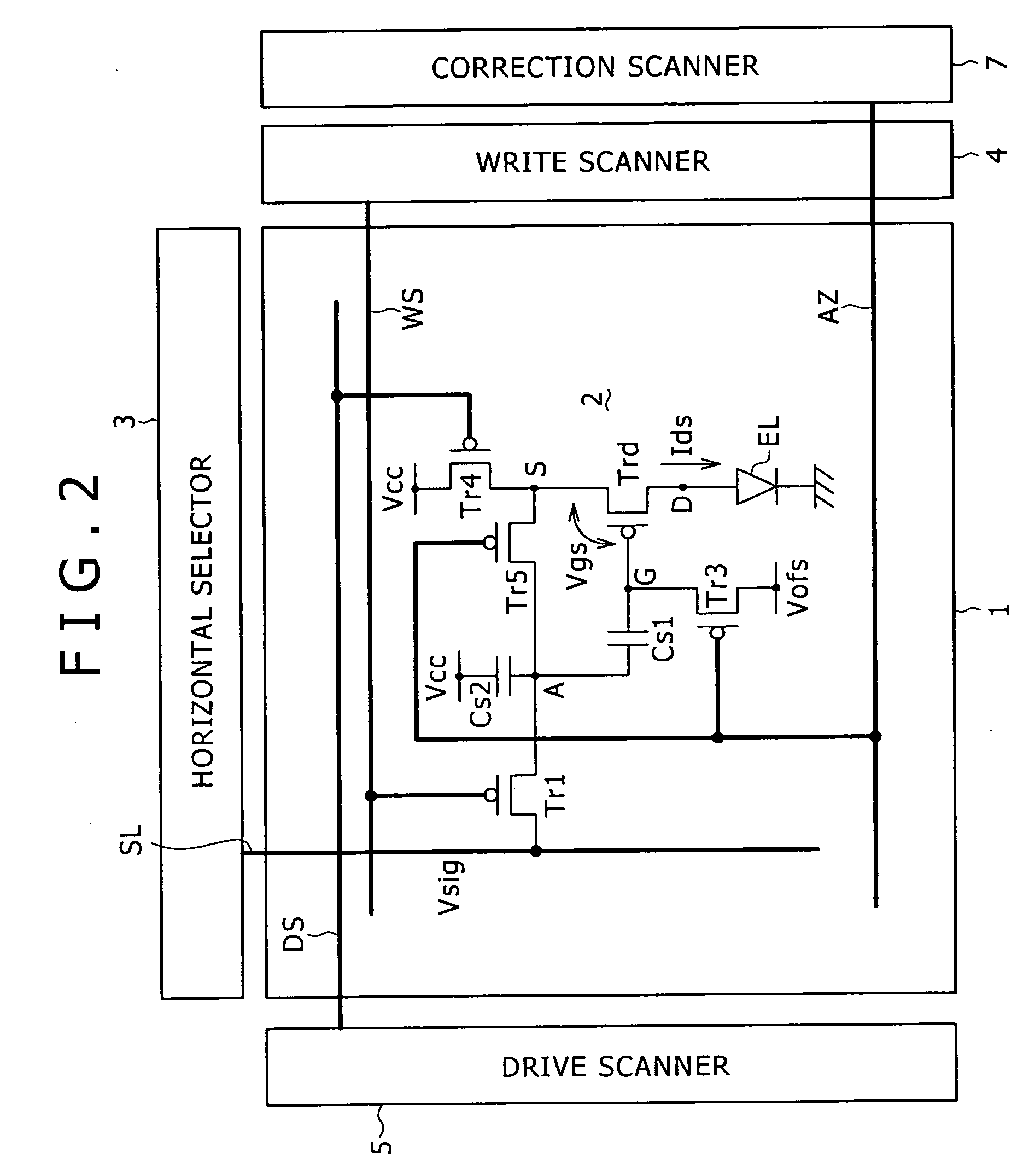
[0033] Embodiments of the present invention will be described below in detail with reference to the accompanying drawings. Initially, in order to clearly show the background of the invention, a reference example of an active-matrix display having a function of correcting the threshold voltage Vth will be described with reference to FIG. 1. Referring to FIG. 1, the active-matrix display includes a pixel array 1 that is a major part, and a peripheral circuit part. The peripheral circuit part includes a horizontal selector 3, a write scanner 4, a drive scanner 5, a correction scanner 7, and so on. The pixel array 1 includes pixels R, G and B that are disposed at the intersections between row scan lines WS and column signal lines SL, and thus are arranged in a matrix. Although pixels of three primary colors of RGB are used to allow color displaying in the example, the present invention is not limited thereto. Each of the pixels R, G and B is formed of a pixel circuit 2. The signal lines...


PUM


Abstract

The invention provides a pixel circuit that can cancel the influence of the mobility of a drive transistor. A drive transistor supplies to a light-emitting element, an output current dependent upon an input voltage during a certain emission period. The light-emitting element emits light with a luminance dependent upon a video signal in response to the output current supplied from the drive transistor. The pixel circuit includes a correction unit that corrects the input voltage held by a capacitive part before the emission period or at the beginning of the emission period, in order to cancel the dependence of the output current on the carrier mobility. The correction unit operates during part of a sampling period in response to control signals supplied from scan lines. Specifically, the correction unit extracts the output current from the drive transistor while the video signal is sampled, and negatively feeds back the output current to the capacitive part to thereby correct the input voltage.

Description

CROSS REFERENCES TO RELATED APPLICATIONS [0001] The present invention contains subject matter related to Japanese Patent Application JP 2005-027028 filed in the Japanese Patent Office on Feb. 2, 2005, the entire contents of which being incorporated herein by reference. BACKGROUND OF THE INVENTION [0002] The present invention relates to a pixel circuit for current-driving a light-emitting element provided for each pixel. The invention also relates to a display that includes the pixel circuits arranged in a matrix (in rows and columns), and particularly to an active-matrix display that employs insulated-gate field effect transistors provided in the respective pixel circuits and controlling the amount of a current applied to a light-emitting element, such as an organic electro-luminescence (EL) element. [0003] In an image display, e.g., in a liquid crystal display, a number of liquid crystal pixels are arranged in a matrix, and the transmittance intensity or reflection intensity of inc...

Claims


Application Information

Patent Timeline
Patent Type & Authority Applications(United States)
IPC IPC(8): G09G3/30H05B44/00
CPCG09G3/3233G09G2300/0819G09G2300/0842G09G2320/045G09G2300/0861G09G2310/061G09G2320/043G09G2300/0852H05B3/347H05B3/08G09G3/3266G09G5/10G09G5/18
Inventor YAMASHITA, JUNICHIUCHINO, KATSUHIDE
Owner SONY CORP
Why Eureka
Try Eureka