Method for forming an aluminum contact

a technology of aluminum contact and aluminum film, which is applied in the direction of semiconductor devices, semiconductor device details, electrical equipment, etc., can solve the problems of difficult forming of metal contacts, cvd may have abnormal growth characteristics in thick aluminum films, and may fail, so as to prevent junction breakdown and reduce resistance , the effect of rapid thermal process

Inactive Publication Date: 2006-06-29
DONGBU ELECTRONICS CO LTD
View PDF7 Cites 0 Cited by
  • Summary
  • Abstract
  • Description
  • Claims
  • Application Information

AI Technical Summary

Benefits of technology

[0024] The exemplary embodiment of the present invention includes forming a barrier metal layer, forming an aluminum layer having low resistivity by using a CVD method, implanting ions (e.g., Bi ions) that are heavier than tungsten, and annealing by using a rapid thermal process. Consequently, a junction breakdown can be prevented by suppressing hillock formation caused by stress in the aluminum layer.

Problems solved by technology

However, the blanket deposition process of Al-CVD may have an abnormal growth characteristic in a thick aluminum film.
Consequently, the film may have a rough surface and may fail to fill a small contact due to blocking of an inlet portion.
This process can be used for a limited region such as a via contact, but it has a difficulty in forming a metal contact wherein a barrier metal is pre-deposited.
As the line width in a circuit becomes narrower, conventional deposition methods for aluminum wiring in a semiconductor device face limitations.
In manufacturing a next generation memory device, the contact hole has a high aspect ratio, so a PVD method (i.e., a sputtering method) becomes insufficient for a deposition process for forming a metal layer having a line width of under 0.25 μm.
However, as the integration of semiconductor devices become higher, a metal having a low resistivity is highly required.
Aluminum having a low resistivity has a difficulty in suppressing a hillock, and thus junction breakdown may occur.

Method used


Image

  • Method for forming an aluminum contact
  • Method for forming an aluminum contact
  • Method for forming an aluminum contact

Examples


Embodiment Construction

[0027] An exemplary embodiment of the present invention will hereinafter be described in detail with reference to the accompanying drawings.

[0028]FIG. 2A to FIG. 2D are cross-sectional views showing principal stages of forming an aluminum contact according to an exemplary embodiment of the present invention.

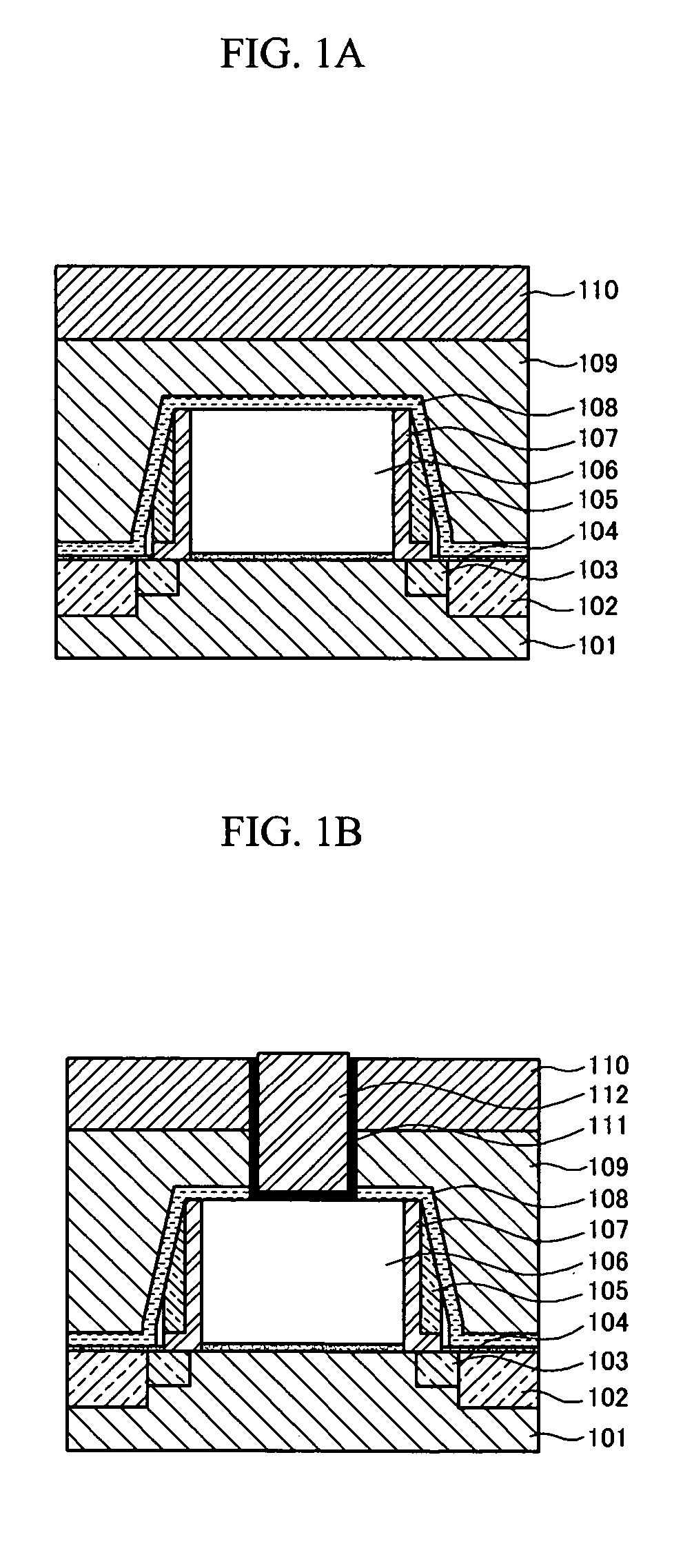
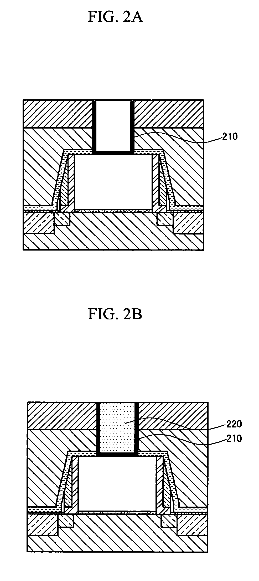
[0029] First, as shown in FIG. 2A, a barrier metal layer 210 is formed on the interlayer insulation layer pattern defining a contact hole so as to form an aluminum layer only in a contact hole. The barrier metal layer 210 can be composed of titanium nitride (TiN), tantalum nitride (TaN), titanium aluminum nitride (TiAlN), titanium silicon nitride (TiSiN), tantalum aluminum nitride (TaAlN), tantalum silicon nitride (TaSiN), tungsten nitride (WN), or a combination thereof.

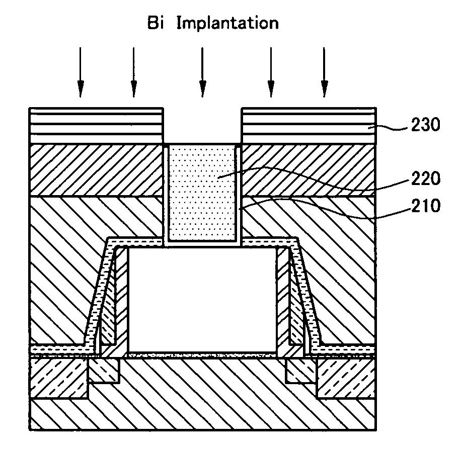
[0030] Subsequently, as shown in FIG. 2B, an aluminum layer 220 is formed on the barrier metal layer 210 by a CVD method so as to fill the contact hole. The aluminum metal layer 220 is planarized by using a che...


PUM

PropertyMeasurementUnit
widthaaaaaaaaaa
thicknessaaaaaaaaaa
aspect ratioaaaaaaaaaa

Abstract

A method of forming an aluminum contact including forming a barrier metal layer on an interlayer insulation layer pattern defining a contact hole, and forming an aluminum layer on the barrier metal layer so as to fill the contact hole. The method further includes forming a photoresist pattern for ion implantation, implanting ions into the aluminum layer, and annealing by using a rapid thermal process.

Description

CROSS-REFERENCE TO RELATED APPLICATION [0001] This application claims priority to and the benefit of Korean Patent Application No. 10-2004-0115518 filed in the Korean Intellectual Property Office on Dec. 29, 2004, the entire contents of which are incorporated herein by reference. BACKGROUND OF THE INVENTION [0002] (a) Field of the Invention [0003] The present invention relates to a method of manufacturing semiconductor devices. More particularly, the present invention relates to a method for forming an aluminum contact in a semiconductor device. [0004] (b) Description of the Related Art [0005] As semiconductor devices have been more highly integrated, width and thickness of metal lines therein have been reduced, and size of a contact has been reduced. Therefore, an aspect ratio of a contact hole has been increased, and thus a method for fully filling the contact hole has become very important. [0006] For a method for fully filling the contact hole having a high aspect ratio with a l...

Claims


Application Information

Patent Timeline
Patent Type & Authority Applications(United States)
IPC IPC(8): H01L21/44
CPCH01L21/76886H01L23/53223H01L2924/0002H01L2924/00H01L21/28H01L21/768
Inventor LEE, JAE-SUK
Owner DONGBU ELECTRONICS CO LTD
Why Eureka
Try Eureka