
Voltage-controlled magnetization reversal writing type magnetic random access memory device and method of writing and reading information using the same

a random access memory, voltage-controlled technology, applied in information storage, static storage, digital storage, etc., can solve the problems of inability to develop ultra-high-integrated memory, difficult to deposit insulating thin film, and inability to develop ferromagnetic semiconductors that can be practically used at room temperatur

Active Publication Date: 2006-06-22
KOREA ADVANCED INST OF SCI & TECH
View PDF2 Cites 55 Cited by
  • Summary
  • Abstract
  • Description
  • Claims
  • Application Information

AI Technical Summary

Benefits of technology

[0016] Accordingly, the present invention has been made keeping in mind the above problems occurring in the prior art, and an object of the present invention is to provide a voltage-controlled magnetization reversal writing type MRAM device and a method of writing and reading information using the MRAM memory device, which allow voltage to be uninterruptedly applied to a Lead-Zirconate-Titanate (PZT) thin film using two base electrodes composed of positive (+) and negative (−) electrodes but also allows writing and reading to be performed independently of each other through the two writing lines and the two reading lines, thus improving the speed of the MRAM device and not requiring a nano-thickness tunneling barrier used in an existing MRAM device, which use materials and structures that facilitate integration with CMOS circuits, thus having excellent advantages from the points of view of the integration of MRAM devices with existing CMOS circuits, memory speed and productivity, which do not require the generation of an external magnetic field, unlike an existing external magnetic field-induced writing type MRAM device, thus enabling low power design, which improve a voltage application scheme, thus allowing an MRAM device to be more effectively manufactured, and which is applied to voltage controlled spin devices as well as memory devices, thus being applicable to the development of ultra high-density next generation memory.
[0019] The electrically conductive base electrodes, the insulation layer, the piezoelectric layer and the Si substrate are made of materials that minimize lattice mismatch therebetween and enable epitaxial growth.

Problems solved by technology

However, in the above-described writing scheme using an externally applied magnetic field, the localization of the magnetic field is not easy, so that there is a fundamental limitation in the development of ultra high-integrated memory.
This acts as a great weak point in the production of MRAM devices because it is difficult to deposit the insulating thin film, which is formed to a constant thickness of 1 nm, on a wafer having a radius of a predetermined number of inches in a production process, and because a precise work is required for the production of MRAM devices.
In the case of the above-described method, there is a problem in that a ferromagnetic semiconductor that can be practically used at room temperature has not been developed to date.
Meanwhile, a method of controlling magnetization reversal by applying voltage to a ferromagnetic thin film is described in US Pat. No. 2003 / 0103371 A1, entitled “Method of Controlling Magnetization Easy Axis in ferromagnetic Films Using Voltage, Ultra High-density, Low Power, Nonvolatile Magnetic Memory Using The Control Method, and Method of Writing Information on The Magnetic Memory.” However, this method uses materials and structures that interfere with the integration of MRAM devices having existing CMOS circuits, so that there is also a problem in that the design is not suitable for ultra high speed MRAM.

Method used


Image

  • Voltage-controlled magnetization reversal writing type magnetic random access memory device and method of writing and reading information using the same
  • Voltage-controlled magnetization reversal writing type magnetic random access memory device and method of writing and reading information using the same
  • Voltage-controlled magnetization reversal writing type magnetic random access memory device and method of writing and reading information using the same

Examples


Embodiment Construction

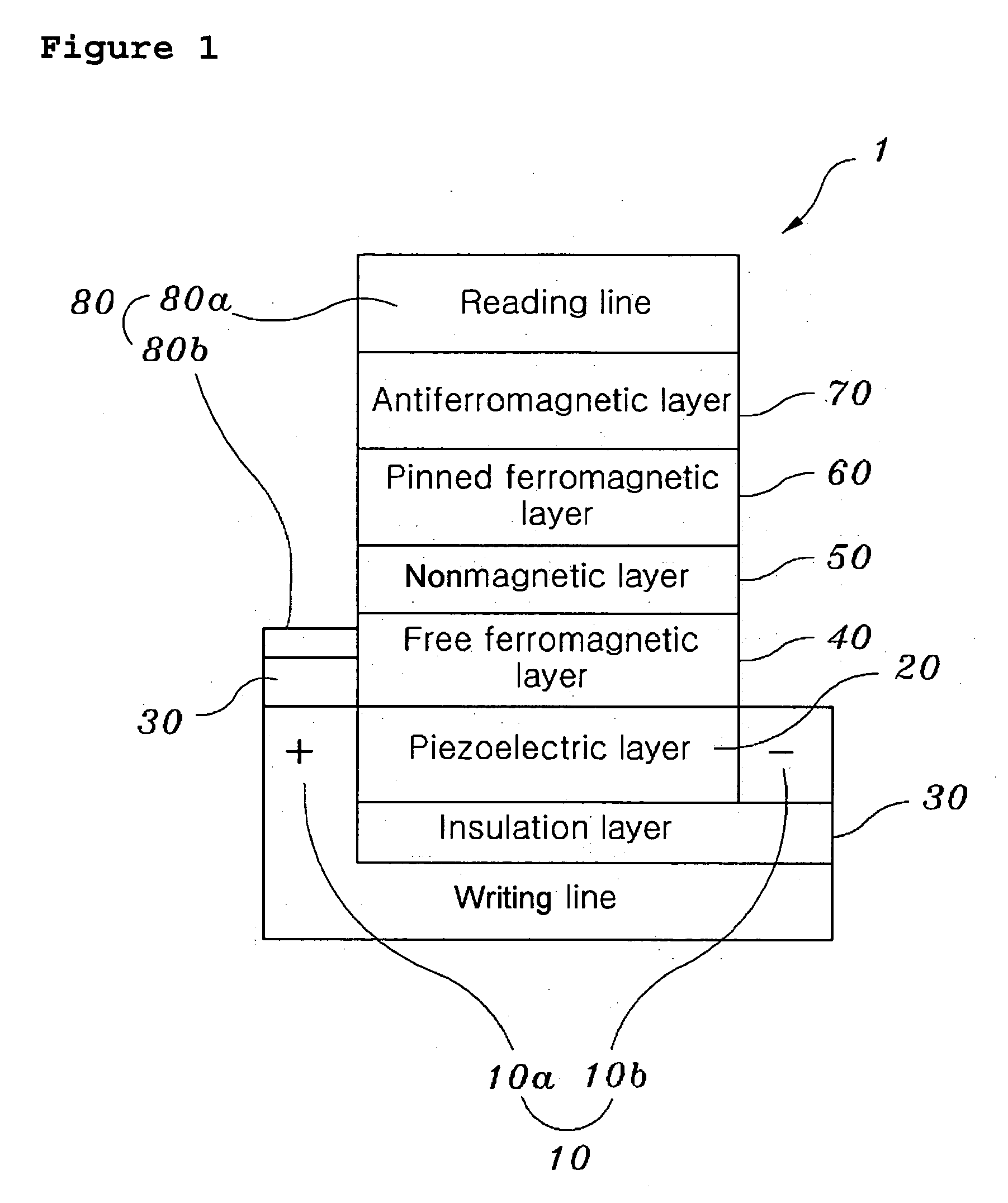
[0047] An embodiment of the present invention is described in detail with reference to the accompanying drawings. FIG. 1 is a schematic sectional view showing the ferromagnetic and piezoelectric layers of a voltage-controlled magnetization reversal writing type MRAM in accordance with the present invention.

[0048] As shown in FIG. 1, the voltage-controlled magnetization reversal writing type MRAM device 1 in accordance with the present invention includes a piezoelectric layer 20, an insulation layer 30, a free ferromagnetic layer 40, a nonmagnetic layer 50, a pinned ferromagnetic layer 60, an antiferromagnetic layer 70, two electrically conductive reading lines 80, and electrically conductive base electrodes 10 having positive (+) and negative (−) electrodes.

[0049] In the MRAM device 1, a SrRuO3 metallic oxide electrode layer is deposited on a Si substrate, thus allowing electrically conductive base electrodes 10 to be formed of SrRuO3.

[0050] The electrically conductive base elect...


PUM


Abstract

A voltage-controlled magnetization reversal writing type Magnetic Random Access Memory (MRAM) device. The MRAM device includes electrically conductive base electrodes, a piezoelectric layer, an insulation layer, a free ferromagnetic layer, a nonmagnetic layer, a pinned ferromagnetic layer, an antiferromagnetic layer and two electrically conductive reading lines. The electrically conductive base electrodes are provided with two writing lines having positive and negative electrodes. The left and right surfaces of piezoelectric layer are disposed to abut the writing lines of the electrically conductive base electrodes, respectively. The insulation layer is disposed beneath the piezoelectric layer and is formed to separate the positive and negative electrodes. The free ferromagnetic layer is disposed on the insulation layer. The nonmagnetic layer is disposed on the free ferromagnetic layer. The pinned ferromagnetic layer is disposed on the nonmagnetic layer. The antiferromagnetic layer is disposed on the pinned ferromagnetic layer. The two electrically conductive reading lines are formed to be perpendicular to each other.

Description

BACKGROUND OF THE INVENTION [0001] 1. Field of the Invention [0002] The present invention relates generally to the design of a new type of next-generation memory device, that is, a magnetic random access memory device, that uses voltage-controlled magnetization reversal and giant magnetoresistance phenomena as a method of writing and reading information to and from memory, and performs writing and reading independently of each other and, more particularly, to a nonvolatile, ultra highly-integrated and super power-saving voltage-controlled magnetization reversal writing type magnetic random access memory device and a method of writing and reading information using the magnetic random access memory device, in which voltage is uninterruptedly applied to a lead-zirconate-titanate thin film using two base electrodes composed of positive (+) and negative (−) electrodes, reading and writing are performed independently of each other using two writing lines and two reading lines, and writing...

Claims


Application Information

Patent Timeline
IPC IPC(8): G11C11/00
CPCG11C11/15G11C5/025H10N50/10H10N50/85
Inventor SHIN, SUNG-CHULJEONG, JONG-RYULVISWAN, RAVINDRANATH
Owner KOREA ADVANCED INST OF SCI & TECH
Learn More