
Surface acoustic wave device and method of manufacturing a surface acoustic wave device

a surface acoustic wave and a manufacturing method technology, applied in piezoelectric/electrostrictive devices, piezoelectric/electrostrictive/magnetostrictive devices, semiconductor devices, etc., can solve the problems of degrading the performance insufficient dimensional accuracy, and inability to ensure the flatness of the surface of the surface acoustic wave element region, so as to achieve good dimensional accuracy, reduced

Inactive Publication Date: 2006-06-22
SEIKO EPSON CORP
View PDF4 Cites 3 Cited by
  • Summary
  • Abstract
  • Description
  • Claims
  • Application Information

AI Technical Summary

Benefits of technology

[0007] In view of the above technical background, an advantage of the present invention is to provide a surface acoustic wave device, which is equipped with an IC region and a surface acoustic wave element region in a semiconductor substrate and is configured as a single chip, and a method of manufacturing the surface acoustic wave device capable of ensuring evenness of the surface acoustic wave element region, and thus obtaining superior characteristics.
[0008] A surface acoustic wave device according to an aspect of the invention includes at least an IC region and a surface acoustic wave element region in a semiconductor substrate and is formed as a single chip, and includes in the IC region a semiconductor element layer having a semiconductor element and an element insulating film formed to cover the semiconductor element and extending to the surface acoustic wave element region, a wiring layer formed by stacking, on the semiconductor element layer, wiring for establishing connection with the semiconductor element and a wiring insulating film extending to the surface acoustic wave element region and for insulating the wiring, a piezoelectric thin film formed above the wiring insulating film. And the surface acoustic wave device further includes, in the surface acoustic wave element region, a surface acoustic wave element formed on the piezoelectric thin film and equipped with an IDT electrode provided with a plurality of electrode fingers, and at least one layer of layer thickness adjusting films having linear shapes and arranged in parallel to the electrode fingers of the IDT electrode and with the same pitch as the electrode fingers of the IDT electrode. The layer thickness adjusting films are formed above the semiconductor substrate, the element insulating film, or the wiring insulating film, and below an area in which the surface acoustic wave element is formed.
[0009] According to this configuration, the step between the IC region and the surface acoustic wave element region can be reduced by providing the layer thickness adjusting films on the semiconductor substrate, the element insulating film, or the wiring insulating film in the surface acoustic wave element region, thus evenness of the surface acoustic wave element region can be ensured. Further, the diffused reflection of the surface acoustic wave excited by the IDT electrodes can be prevented by providing the layer thickness adjusting films having linear shapes substantially in parallel to and with the same pitch as the electrode fingers of the IDT electrodes.
[0010] As described above, the surface acoustic wave element can be formed in the even surface acoustic wave element region to form the IDT electrodes with good dimensional accuracy to reduce variation in the resonant frequency of the surface acoustic wave element, and further to prevent the diffused reflection of the surface acoustic wave, thus the surface acoustic wave device with superior characteristics can be provided.
[0011] In the surface acoustic wave device according to another aspect of the invention, the layer thickness adjusting films are formed in the same pitch as the pitch of the electrode fingers with respect to positions where the center lines of the electrode fingers in the line width direction match the respective center lines of the layer thickness adjusting films in the line width direction. According to this configuration, the diffused reflection of the surface acoustic wave can effectively be prevented, thus providing the surface acoustic wave element with good characteristics.
[0012] In the surface acoustic wave device according to still another aspect of the invention, the width of each of the electrode fingers is equal to the width of respective one of the layer thickness adjusting films. According to this configuration, the diffused reflection of the surface acoustic wave can further effectively be prevented, thus providing the surface acoustic wave element with good characteristics.

Problems solved by technology

Typically, in case of such a surface acoustic wave device, a large number of surface acoustic wave devices are formed in a semiconductor wafer so as to border on each other, and as layers such as the insulating layer are stacked, the step inclines and advances to the surface acoustic wave element region, this causes a problem that the flatness of the surface of the surface acoustic wave element region cannot be assured.
If the flatness of the surface is not sufficient, the surface acoustic wave element cannot be manufactured with sufficient dimensional accuracy, which degrades the performance of the surface acoustic wave element.
Further, the unevenness of the surface caused by the insufficient flatness causes a variation in the thickness of the piezoelectric thin film formed thereon, and a variation in the resonant frequency of the surface acoustic wave element is concerned.

Method used


Image

  • Surface acoustic wave device and method of manufacturing a surface acoustic wave device
  • Surface acoustic wave device and method of manufacturing a surface acoustic wave device
  • Surface acoustic wave device and method of manufacturing a surface acoustic wave device

Examples


first embodiment

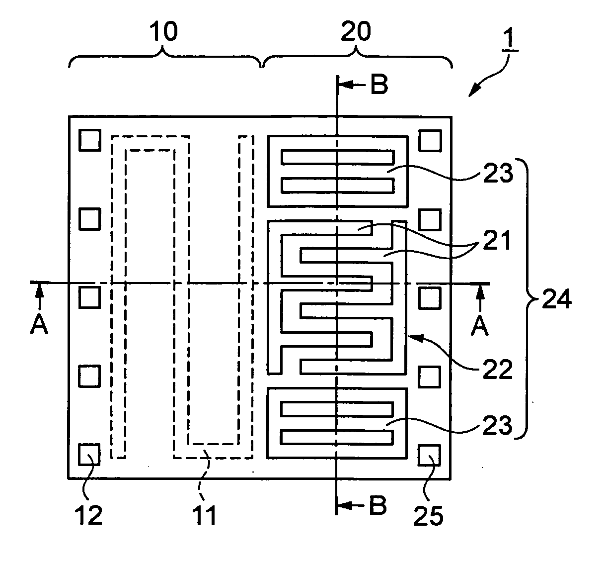
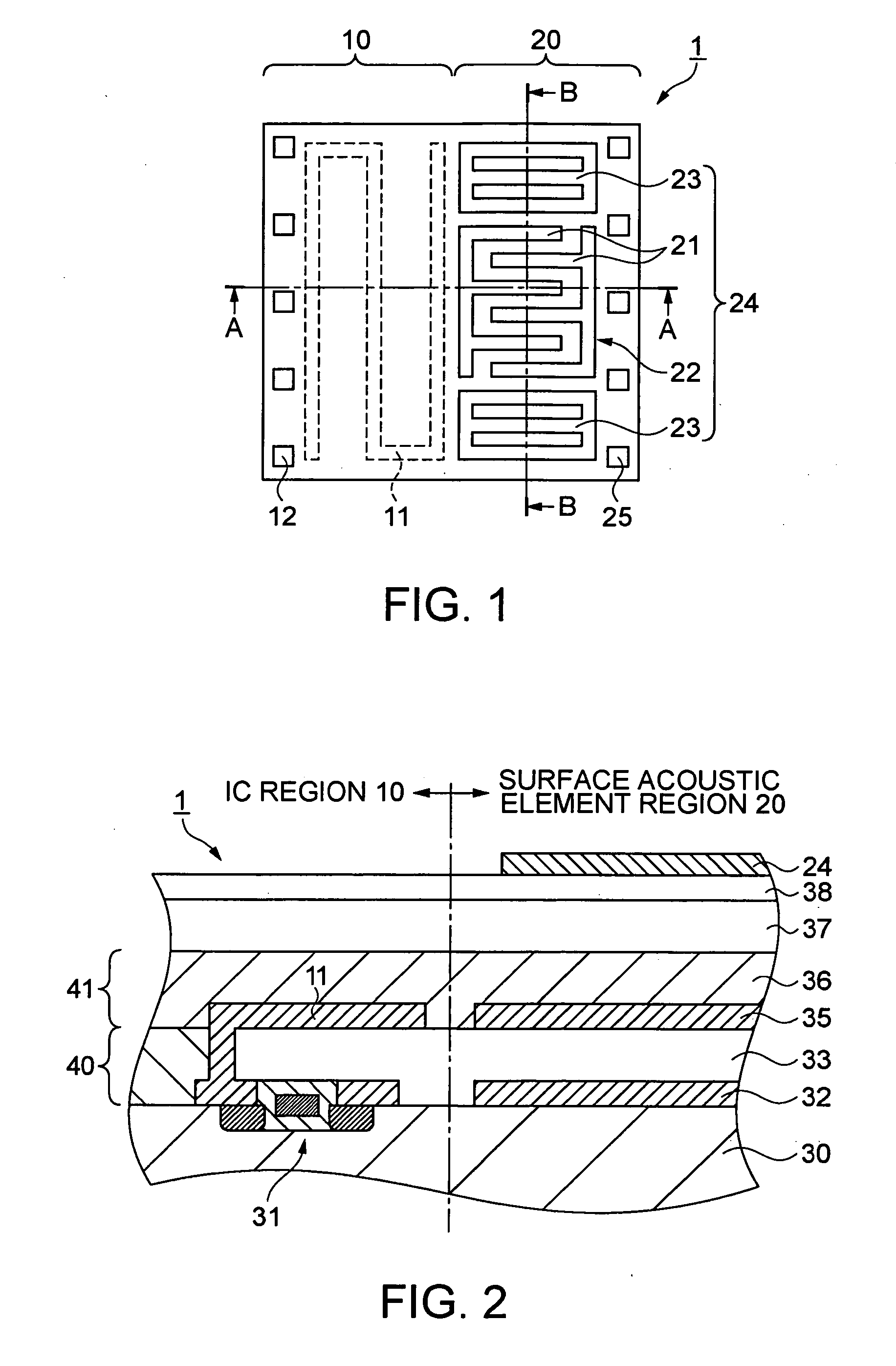
[0031]FIG. 1 is a schematic plan view showing a surface acoustic wave device according to an embodiment of the invention. A surface acoustic wave device 1 is provided with an IC region 10 and a surface acoustic wave element region 20 in a semiconductor substrate. In the IC region, a semiconductor element (shown in FIG. 2) is formed on the semiconductor substrate, and Al wiring 11 for connecting the semiconductor element is stacked thereon. And, Al pads 12 are provided for electrical connection with the outside. Further, a high-frequency circuit such as an oscillator circuit for driving the surface acoustic wave element 24 is included in the IC region 10.

[0032] In the surface acoustic wave element region 20, there is formed a SAW resonator as the surface acoustic wave element 24 equipped with IDT electrodes 22 and reflectors 23. The IDT electrodes 22 are equipped with electrode fingers 21 disposed so as to alternately engage with each other. And, Al pads 25 are provided for electric...

second embodiment

[0050] Hereinafter, a method of manufacturing the surface acoustic wave device will be described. FIGS. 7A through 7D are views for explaining processes showing a method of manufacturing the surface acoustic wave device according to an embodiment of the invention, and the processes proceed in the order from 7A to 7D.

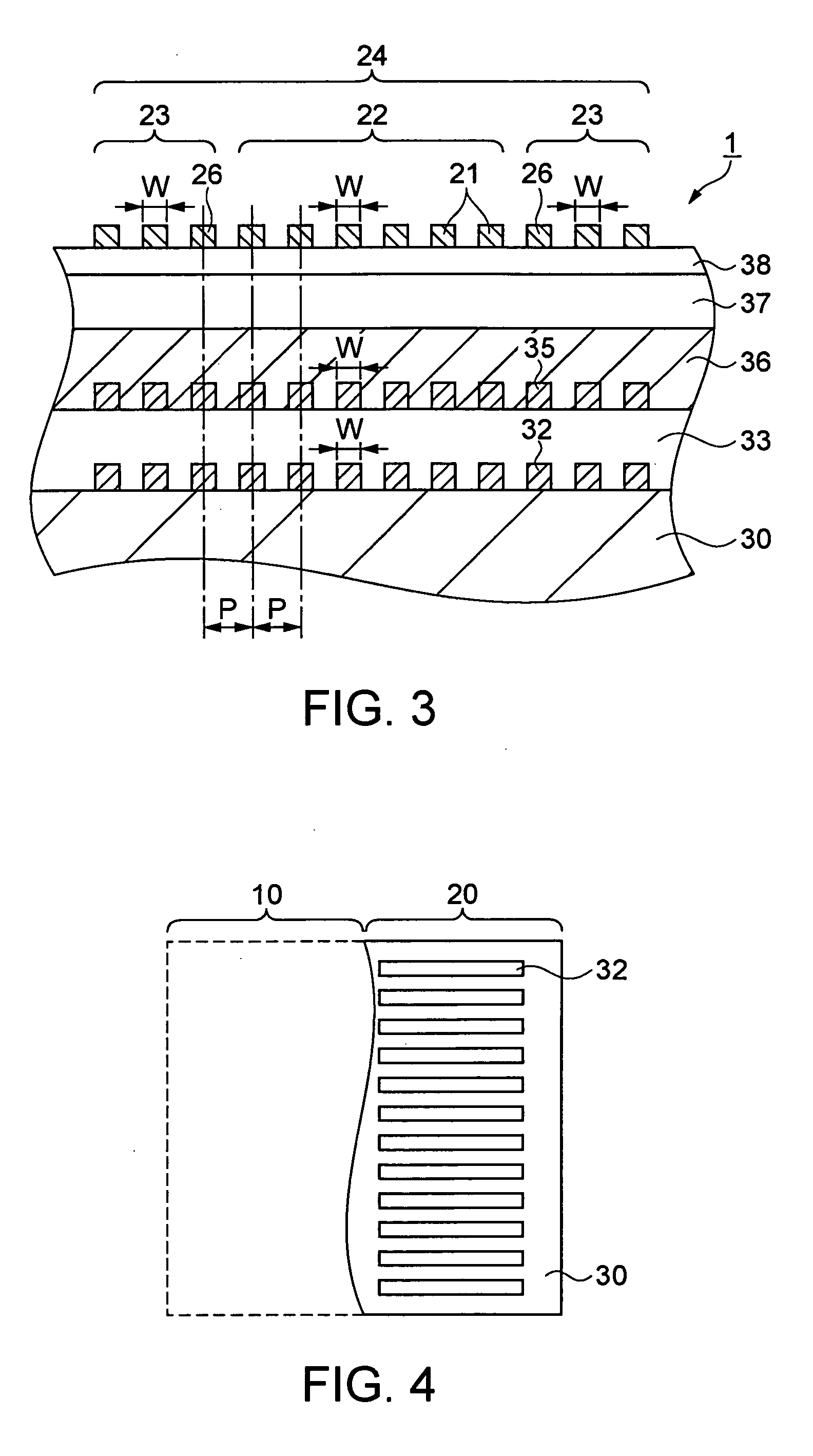
[0051] In FIG. 7A, using a known method, a large number of semiconductor elements 31 are formed in the IC region 10 on the semiconductor substrate 30 made of silicon. Further, the first layer thickness adjusting films 32 made of Al are formed in the surface acoustic wave element region 20 on the semiconductor substrate 30. The first layer thickness adjusting films 32 are formed linearly and substantially in parallel to the electrode fingers of the IDT electrode of the surface acoustic wave element, as shown in FIG. 4. Further, the first layer thickness adjusting films 32 are formed to have the same pitch and the same line width as the electrode fingers of the IDT electr...

third embodiment

[0059] Hereinafter, modified examples of the method of manufacturing the surface acoustic wave device will be described. The element insulating film 33 shown in FIG. 2 or FIG. 7B is often formed using a vapor phase process in response to a higher frequency or finer pitch wiring. However, in the case of a relatively low frequency of no higher than several hundreds MHz, the previous-generation wiring of no smaller than 0.35 μm can be adopted. In this case, by applying SOG to the element insulating film 33, a more low-cost film forming process can be provided. Note that, in the SOG process, liquid glass is deposited on a wafer by spin-coating in a preliminary rotational speed of 300 rpm for 3 seconds, and then in a main rotational speed of 300 rpm for 10 seconds. After then, it is processed in a baking oven at 80° C. for 3 minutes, and finally cured at 300° C. for 60 minutes to be completed.

[0060] As described above, according to the method of manufacturing the surface acoustic wave d...


PUM


Abstract

A surface acoustic wave device including at least an IC region and a surface acoustic wave element region in a semiconductor substrate and formed as a single chip, including, in the IC region, a semiconductor element layer having a semiconductor element and an element insulating film formed to cover the semiconductor element and extending to the surface acoustic wave element region, a wiring layer formed by stacking, on the semiconductor element layer, wiring for establishing connection with the semiconductor element and a wiring insulating film extending to the surface acoustic wave element region and for insulating the wiring, and a piezoelectric thin film formed above the wiring insulating film, and in the surface acoustic wave element region, a surface acoustic wave element formed on the piezoelectric thin film and equipped with an IDT electrode provided with a plurality of electrode fingers, and at least one layer of layer thickness adjusting films having linear shapes and arranged in parallel to and with the same pitch as the electrode fingers of the IDT electrode, and formed above one of the semiconductor substrate, the element insulating film, and the wiring insulating film, and below an area in which the surface acoustic wave element is formed.

Description

BACKGROUND OF THE INVENTION [0001] 1. Technical Field [0002] The present invention relates to a surface acoustic wave device provided with an IC region and a surface acoustic wave element region on a semiconductor substrate to form a single chip. [0003] 2. Related Art [0004] Surface acoustic wave devices represented by a SAW resonator or a SAW filter have various superior characteristics such as high frequency, compact size, or high mass productivity, and therefore, are widely used in the telecommunications field. In recent years, along with the popularization of mobile telecommunication devices, downsizing and weight saving of components used in the high-frequency area are strongly desired. [0005] To cope with the desire, as shown in a document of J. H. Viseer, IEEE, Ultrasonics Symposium, p.195-200 (1989), for example, there is proposed a surface acoustic wave device having a SAW filter formed by providing a piezoelectric thin film on a semiconductor substrate partially provided w...

Claims


Application Information

Patent Timeline
Patent Type & Authority Applications(United States)
IPC IPC(8): H03H9/25H01L41/08H01L41/09H01L41/187H01L41/22H01L41/311H03H3/08H03H9/145
CPCH03H3/08H03H9/02866H03H9/02976H03H9/145
Inventor FURUHATA, MAKOTOSATO, HISAKATSU
Owner SEIKO EPSON CORP
Learn More