
Method for selective deposition of a thin self-assembled monolayer

Active Publication Date: 2006-06-15
INTERUNIVERSITAIR MICRO ELECTRONICS CENT (IMEC VZW) +1
View PDF5 Cites 346 Cited by
  • Summary
  • Abstract
  • Description
  • Claims
  • Application Information

AI Technical Summary

Benefits of technology

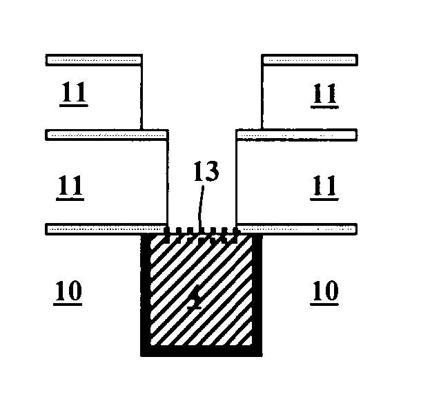
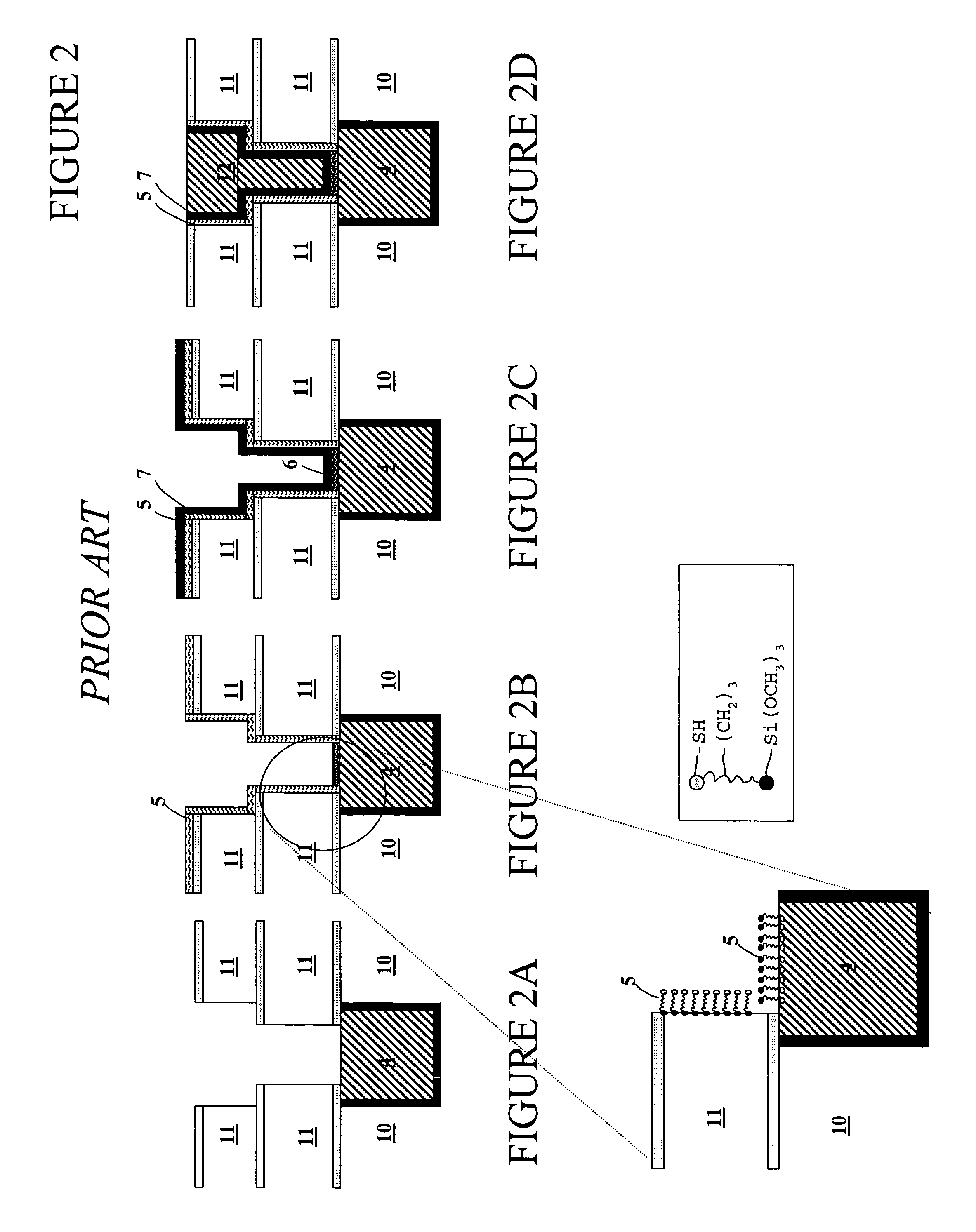
[0011] The preferred embodiments solve the problem of applying a (non-selective) self-assembled monolayers for use as barrier layer in dual damascene structures as described in the prior art by depositing first a protective (sacrificial) self-assembled monolayer (referred to as SAM-1) selectively to the copper surface of an existing metal structure of a dual damascene structure before applying a second (permanent) self-assembled monolayer (referred to as SAM-2) to the non-copper parts of said dual damascene structure. By applying said sacrificial SAM-1 to the already existing copper surface of a dual damascene structure (also referred to as underlying metal layer n-1) said existing copper surface will be protected from non-selective adsorption of SAM-2. The release of the sacrificial SAM-1 after SAM-2 deposition on the dielectric makes it possible to create a good and direct copper to copper contact in the final dual damascene structure or in other words a good Cu—Cu contact between the via bottom (metal n) and the underlying metal (n−1) of a dual damascene structure can be achieved.

Problems solved by technology

One of the major challenges in Cu metallization technology is the prevention of the rapid diffusion of Cu into adjoining layers of SiO2 and related low-dielectric-constant materials (e.g., fluorinated SiOx, SiOCH) during device operation.
This is because Cu incorporation into the dielectric degrades the dielectric properties of the insulating layer, causing increased leakage currents, and leading to inferior device performance and failure.
It is difficult to obtain such thin barriers with acceptable step coverage by conventional metal deposition methods (Plasma Vapor deposition (PVD) or Chemical Vapor Deposition (CVD)) without compromising the barrier-layer microstructure and / or their conformality in high-aspect-ratio features.
Additionally thick diffusion barrier layers take up the volume meant for low-resistivity Cu, reducing the advantages of scaling (miniaturization).
However, to obtain conformal films with thicknesses below 5 nm of conventional barrier materials, it is not clear if they will be effective due to high defectivity.
The use of said SAM layer in integrated circuit structures such as dual damascene structures wherein electrical contact is required between the metal line of interest to metal lines above or below the situation is more complicated.
Deposition of said SAM layer (comprising organo-silane molecules) to the already existing metal structure will lead to poor adhesion of Cu seed layers prior to further Cu deposition and poor electrical conductivity later on in the finalized dual damascene structure.

Method used


Image

  • Method for selective deposition of a thin self-assembled monolayer
  • Method for selective deposition of a thin self-assembled monolayer
  • Method for selective deposition of a thin self-assembled monolayer

Examples


example 1

SAM Preparation and Coating Onto Wafer Substrates by Liquid Immersion

[0057] SAM-1 was prepared by immersion of Cu plated wafer substrates in a dilute solution of 1-decanethiol. The dilute solution was obtained by dilution of 1 ml of concentrated 1-decanethiol in 5000 ml solvent, using isopropyl alcohol (IPA) as solvent at ambient temperature for 2 h. The SAM-1 chemical structure is CH3—(CH2)9—SH, also referred to as C10 or 1-decanethiol. The SAM-1 material has 96% purity and is obtained from Sigma-Aldrich. The C10-modified wafer was then rinsed with copious amounts of IPA (30 sec) and dried under nitrogen. The substrates were then electroplated with copper. The Cu substrates were cleaned by immersion in 3.7% hydrochloric acid for 5 min. followed by rinsing with copious amounts of deionised water (2 min) and then solvent (30 sec) immediately before immersion in thiol solution.

[0058] SAM-2 was prepared by rinsing SiO2 substrate in toluene (10 sec) and then immersion in a dilute solu...

example 2

SAM Preparation and Coating Onto Wafer Substrates by Vapour Deposition

[0060] SAM-1 or SAM-2 can also be adsorbed from the vapour phase. SAM-1 or SAM-2 was contained in a pyrex glass tube and connected via a gas line to a high vacuum system containing the substrate of interest. There was a valve between the vacuum system and the glass tube. By opening this valve, the substrate contained in the vacuum system was exposed to the vapour of SAM-1 or SAM-2 for different times depending on the dosing pressure.

Example 3

Contact Angle (CA) Measurements

[0061] Water CA measurements were used to assess SAM quality, more specifically adhesion properties to the different substrates and thermal stability of the SAM layers. Static contact angles of deionized water deposited on the samples were measured in air using a software-controlled Video Contact Angle System OCA-20 (DataPhysics). All angles measured are subject to an error of ±0.1°. In addition, a variation of ±2.5° was typically observed ac...

example 3

Adhesion Measurements

[0065] Adhesion measurements were made on 4 wafers (indicated as D13, D14, D15 and D16 in Table 2) that continued processing (Cu seed deposition) after the SAM deposition. The adhesion measurements were performed by cleaving 2 sections (cords) from the wafer, applying tape (Scotch “red” crystal clear tape) to the pieces and pulling the tape from the cleaved edge of the wafer. The tape is pulled with a steady motion parallel to the wafer surface. Several (5-6) pieces of tape are attached to the wafer and pulled sequentially. The test was performed on 2 pieces per wafer to get sufficient sample size. Each tape pull is considered a trial. Failure is defined as a test which results in Cu on the tape. The yield is calculated by #_pass / #_trials (%). The results of the adhesion test showed good adhesion properties for SiO2 / SAM-2 / Cu (D16) and a poor adhesion for Cu / SAM-1 / Cu & Cu / SAM-1 / SAM-2 / Cu (D13 & D15).

TABLE 2Adhesion test resultsAdhesionwafersubstrateSAMPasstrial...


PUM


Abstract

A method for selective deposition of self-assembled monolayers to the surface of a substrate for use as a diffusion barrier layer in interconnect structures is provided comprising the steps of depositing a first self-assembled monolayer to said surface, depositing a second self-assembled monolayer to the non-covered parts of said surface and subsequently heating said substrate to remove the first self-assembled monolayer. The method of selective deposition of self-assembled monolayers is applied for the use as diffusion barrier layers in a (dual) damascene structure for integrated circuits.

Description

CROSS-REFERENCE TO RELATED APPLICATIONS [0001] This application claims priority under 35 U.S.C. § 119(e) to U.S. provisional application Ser. No. 60 / 634,900, filed Dec. 9, 2004, the disclosure of which is hereby incorporated by reference in its entirety and is made a portion of this application.FIELD OF THE INVENTION [0002] The present invention is related to the field of semiconductor processing. More specifically it is related to the field of forming self-assembled monolayers for use as diffusion barrier layers. More specifically it is related to field of (e.g. copper) damascene advanced interconnect applications for integrated circuit (IC) manufacturing. BACKGROUND OF THE INVENTION [0003] Copper is the preferred metal for creating multilevel interconnect structures in ultra-large-scale-integrated circuits because of its high electrical conductivity and electromigration resistance. One of the major challenges in Cu metallization technology is the prevention of the rapid diffusion ...

Claims


Application Information

Patent Timeline
IPC IPC(8): H01L21/4763H01L21/31
CPCB82Y30/00B82Y40/00H01L21/28562H01L21/3128H01L21/76807H01L21/76814H01L21/76826H01L21/76831H01L21/76834H01L21/76843H01L21/02126
Inventor WHELAN, CAROLINESUTCLIFFE, VICTOR
Owner INTERUNIVERSITAIR MICRO ELECTRONICS CENT (IMEC VZW)
Learn More