Capacitive coupling plasma processing apparatus
a plasma processing and coupling technology, applied in the direction of electric discharge tubes, chemical vapor deposition coatings, coatings, etc., can solve the problems of poor planar uniformity, charge-up damage, and difficulty in controlling plasma uniformity, so as to prevent charge-up damage and high planar uniformity of plasma processing
- Summary
- Abstract
- Description
- Claims
- Application Information
AI Technical Summary
Benefits of technology
Problems solved by technology
Method used
Image
Examples
first embodiment
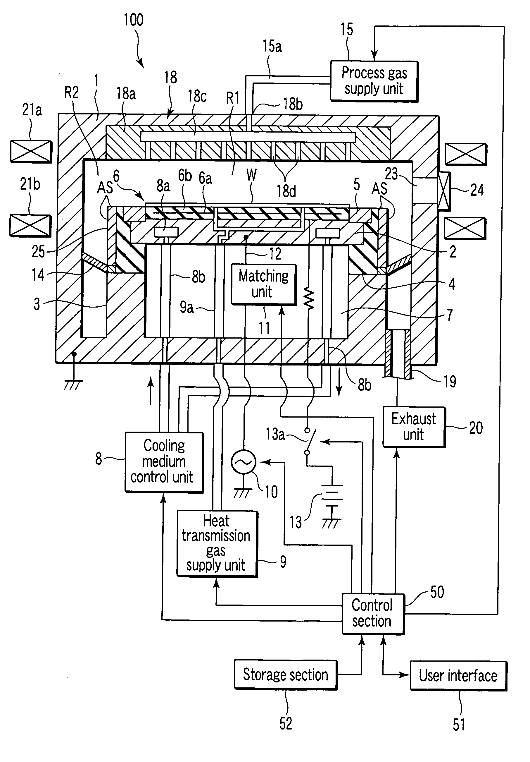
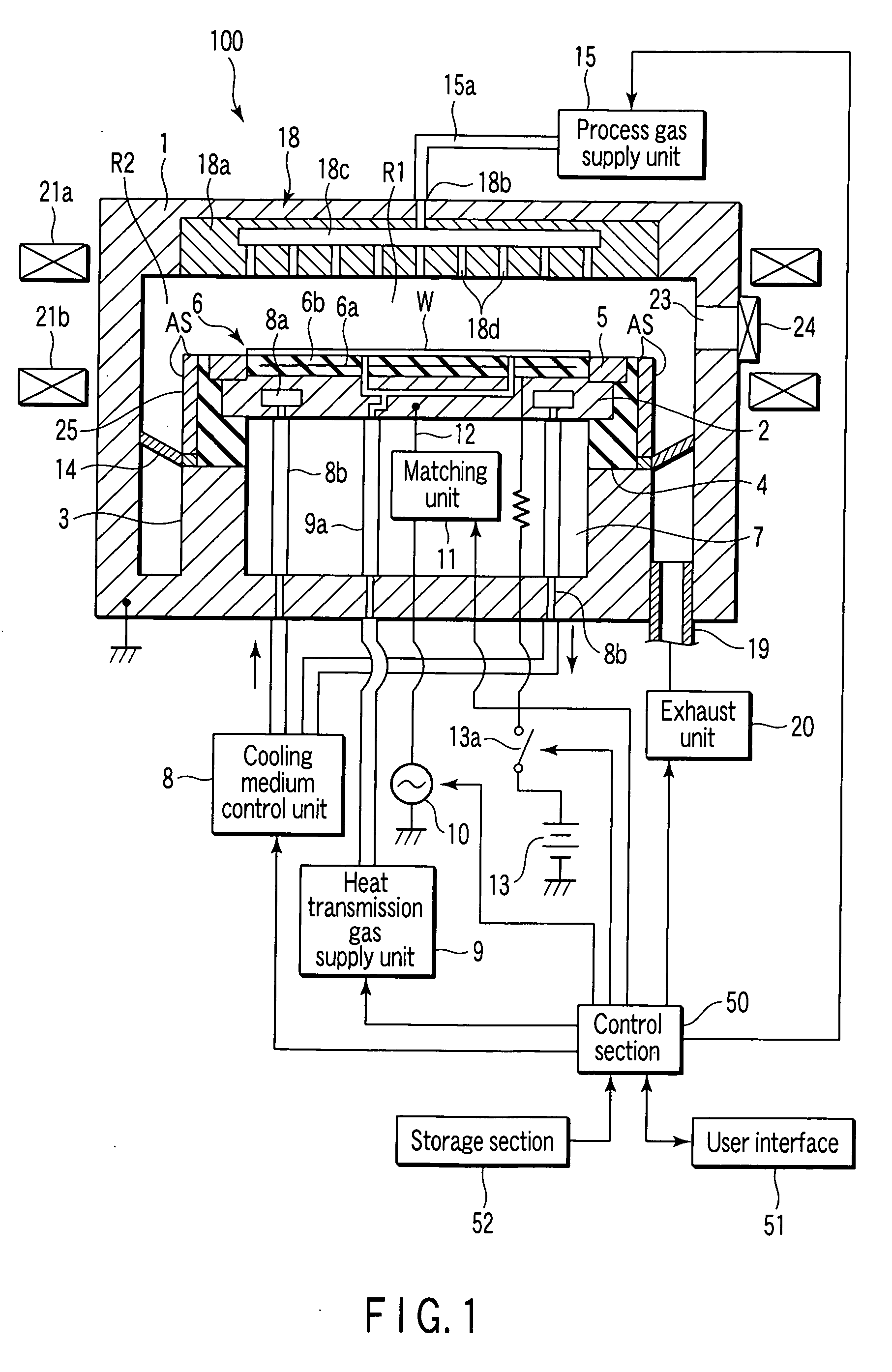
[0044]FIG. 1 is a sectional view showing a plasma etching apparatus as a plasma processing apparatus according to a first embodiment of the present invention. This apparatus is arranged to etch an oxide film (SiO2 film) disposed on a semiconductor wafer.
[0045] This plasma etching apparatus 100 includes an airtight process chamber 1 having an essentially cylindrical shape. For example, the chamber 1 has a main body made of a metal, such as aluminum, with an inner surface covered with an insulating film formed thereon, such as an oxidization processed film, or insulative ceramic film of, e.g. Y2O3 (for example, a thermal spraying film). The chamber 1 is grounded.
[0046] A support table 2 is disposed in the chamber 1 and configured to horizontally support a target substrate or wafer W and to also serve as a lower electrode. For example, the support table 2 is made of aluminum with an oxidization processed surface. A support portion 3 having a ring shape extends upward from the bottom ...
second embodiment
[0090]FIG. 12 is a sectional view showing a plasma etching apparatus as a plasma processing apparatus according to a second embodiment of the present invention. This apparatus is arranged to etch an Si layer or Si substrate surface disposed on a semiconductor wafer. Since the apparatus shown in FIG. 12 has a basic structure essentially the same as that shown in FIG. 1, the following explanation will be given, focusing on the differences.
[0091] This plasma etching apparatus 200 includes a support portion 3 that has a ring shape and extends upward from the bottom of a process chamber 1. An insulating member 4 having a ring shape is disposed on the support portion 3, to support the periphery of a support table 2. A focus ring 35 made of an insulative material, such as SiO2, is placed on the periphery of the top of the support table 2. The insulating member 4, an upper outer surface of the support portion 3, most of the inner surface of the chamber 1, and the surface of the upper elect...
PUM
| Property | Measurement | Unit |
|---|---|---|
| frequency | aaaaa | aaaaa |
| magnetic field | aaaaa | aaaaa |
| magnetic field | aaaaa | aaaaa |
Abstract
Description
Claims
Application Information
 - R&D
- Intellectual Property
- Life Sciences
- Materials
- Tech Scout
- Unparalleled Data Quality
- Higher Quality Content
- 60% Fewer Hallucinations
Browse by: Latest US Patents, China's latest patents, Technical Efficacy Thesaurus, Application Domain, Technology Topic, Popular Technical Reports.
© 2025 PatSnap. All rights reserved.Legal|Privacy policy|Modern Slavery Act Transparency Statement|Sitemap|About US| Contact US: help@patsnap.com


