NROM semiconductor memory device and fabrication method

a technology of semiconductor memory and fabrication method, which is applied in the direction of semiconductor devices, electrical equipment, basic electric elements, etc., can solve the problems of reducing the production of channel hot electrons, and a punch-through from one transistor to an adjacent transistor can aris

Inactive Publication Date: 2006-05-25
QIMONDA
View PDF8 Cites 7 Cited by
  • Summary
  • Abstract
  • Description
  • Claims
  • Application Information

AI Technical Summary

Benefits of technology

[0016] The idea on which the present invention is based involves introducing a concomitantly filled isolation trench between two adjacent u-MOSFETs. A special process sequence can be used to produce the isolation trench in a self-aligned manner. The isolation trench prevents the punch-through between the adjacent transistors and can be set in accordance with the conditions using the depth of the trench. In addition, the isolation trench prevents undesirable injection of hot electrons into the adjacent transistors.
[0023] In accordance with another preferred development, the trenches are configured in an angular manner in the lower trench region, and, before the multilayer dielectric is formed on the trench walls, ions are implanted into the trenches using the hard mask and subsequent implantation is carried out in order to form channel blocking regions in the semiconductor substrate under the trenches. In this other preferred development, the channel blocking regions have the effect that no undesirable field strength effects occur at the corners of these angular u-MOSFETs.

Problems solved by technology

The fact that a punch-through between the drain D and the source S of the respective MOSFET can occur when there are excessively high voltages at the drain, in particular if the transistor has a short channel length of typically less than 250 nm, has proved to be disadvantageous in these known NROM memory cells.
However, initial measurements on NROM semiconductor memory devices of this type have revealed that, in this case, the problem of a punch-through from one transistor to an adjacent transistor can arise, as indicated in FIG. 5 by the arrow PT between the transistors T1″ and T2″.
In addition, a punch-through between the channels may occur, thus reducing the production of channel hot electrons.

Method used


Image

  • NROM semiconductor memory device and fabrication method
  • NROM semiconductor memory device and fabrication method
  • NROM semiconductor memory device and fabrication method

Examples


Embodiment Construction

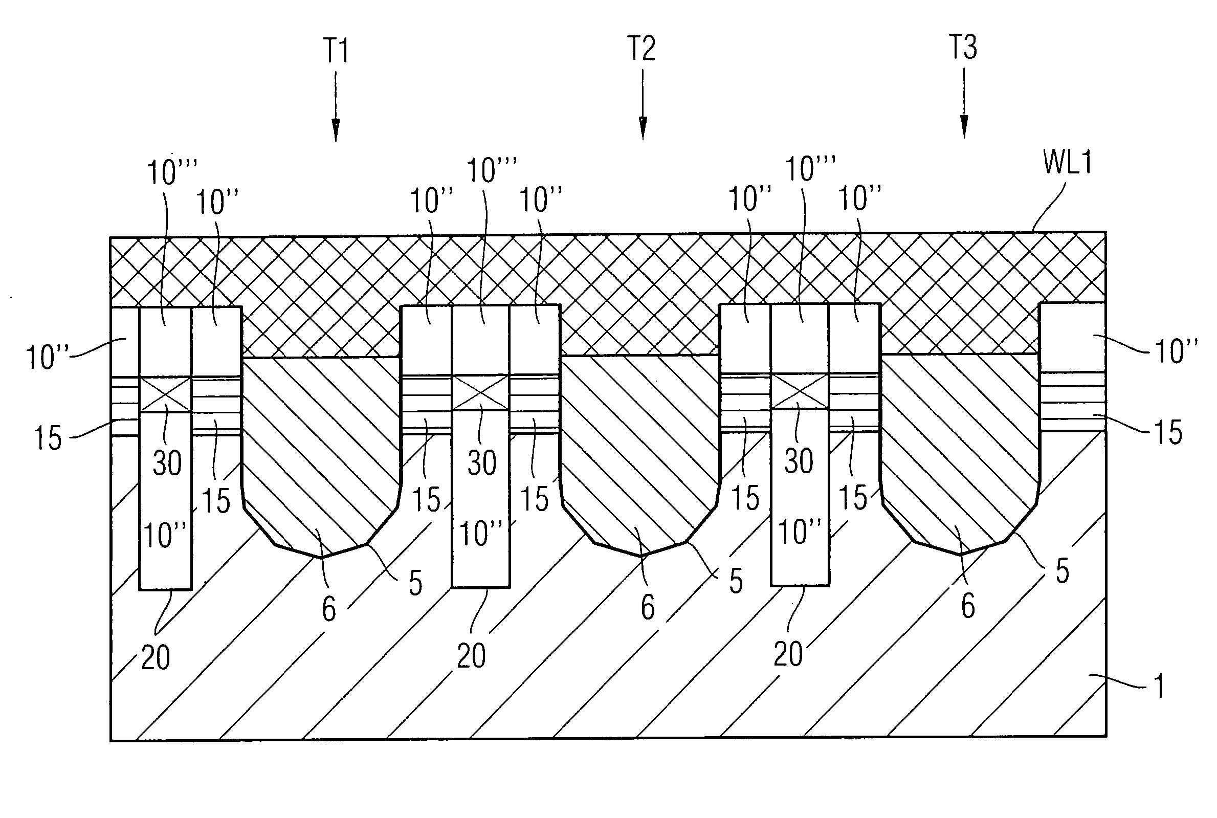
[0030] In the figures, identical reference symbols denote identical or functionally identical components.

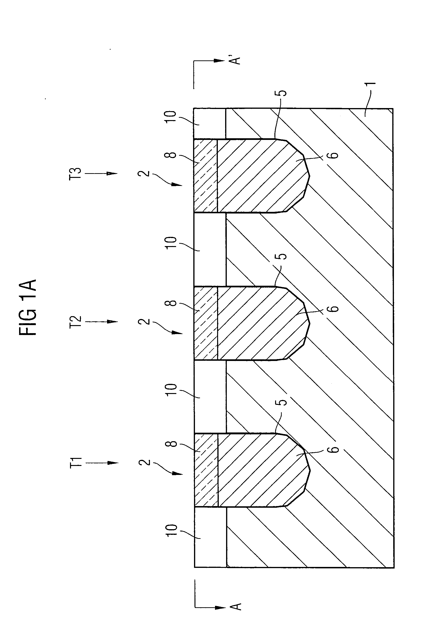
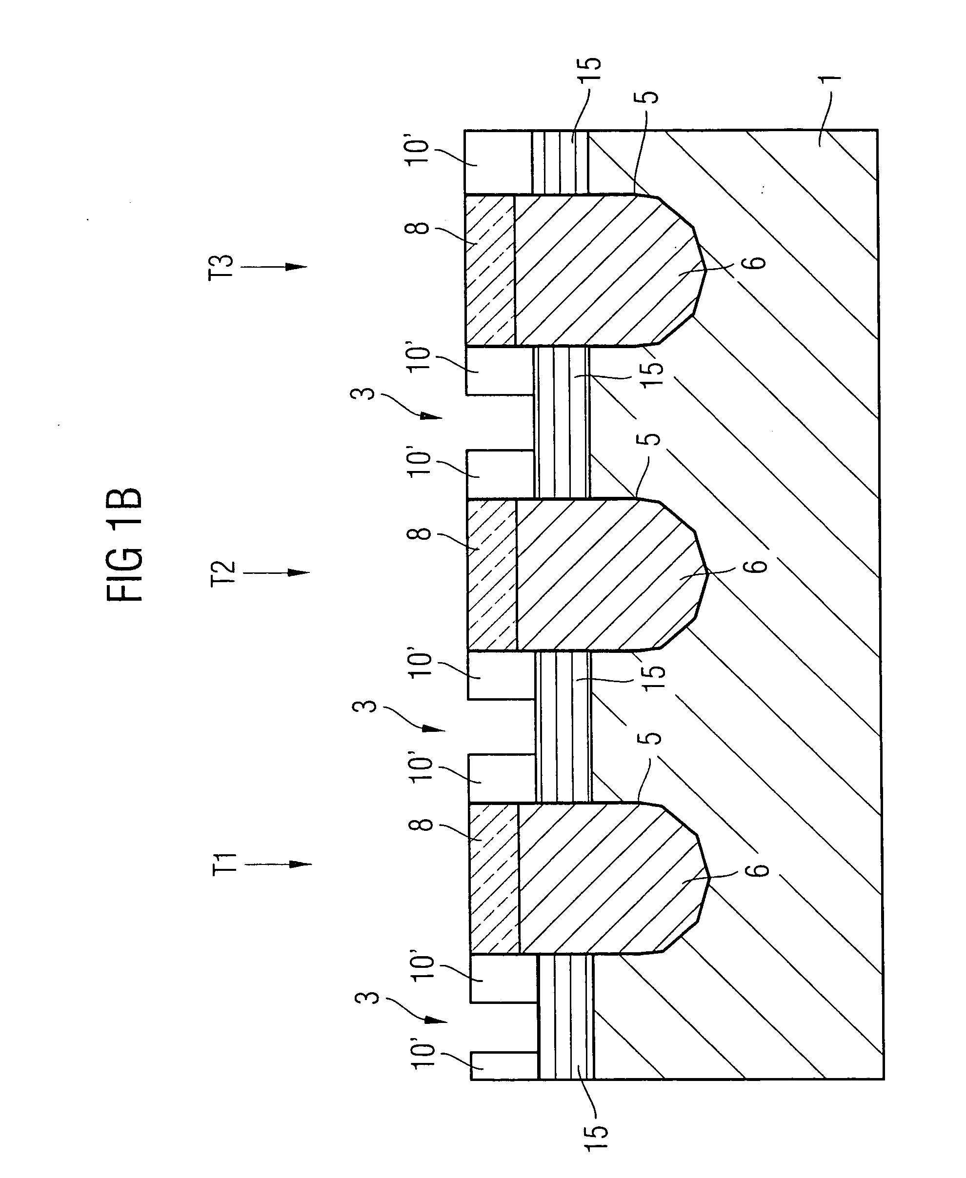
[0031]FIGS. 1a-f show diagrammatic illustrations of successive method stages of a method for fabricating an NROM semiconductor memory device as a first embodiment of the present invention, and FIG. 2 shows a plan view of a cell array having an NROM semiconductor memory device in accordance with the first embodiment of the present invention.

[0032] In FIG. 1a, 1 denotes a p−-type silicon semiconductor substrate on which is situated a hard mask 10 which is made of silicon oxide and has been used to produce transistor trenches 2 (which have a rounded lower trench region) in the substrate 1. Reference symbol 5 denotes the ONO triple dielectric which is situated on the trench walls and on the trench bottom, reference symbol 6 denotes a partial polysilicon filling as a gate, which has been produced by deposition, chemical mechanical polishing and etching back, and reference symbol 8 d...


PUM


Abstract

This invention relates to a method for producing an NROM semiconductor memory device and a corresponding NROM semiconductor memory device. The inventive production method comprises the following steps: a plurality of spaced-apart U-shaped MOSFETS are provided along rows in a first direction and along gaps in a second direction inside trenches of a semiconductor substrate, said U-shaped MOSFETS comprising a multilayer dielectric, especially an ONO dielectric, for trapping charges; source / drain areas are provided between the U-shaped MOSFETS in intermediate spaces located between the rows that extend parallel to the gaps; insulating trenches are provided in the source / drain areas between the U-shaped MOSFETS of adjacent gaps, down to a certain depth in the semiconductor substrate, said insulating trenches cutting up the source / drain areas into respective bit lines; the insulating trenches are filled with an insulating material; and word lines are provided for connecting respective rows of U-shaped MOSFETS.

Description

RELATION APPLICATIONS [0001] This application is a continuation of PCT patent application number PCT / EP2004 / 004772, filed May 5, 2004, which claims priority to German patent application number 10324550.2, filed May 30, 2003, the disclosures of each of which are incorporated herein by reference in their entirety.TECHNICAL FIELD [0002] The present invention relates to a method for fabricating an NROM semiconductor memory device and to a corresponding NROM semiconductor memory device. BACKGROUND ART [0003] NROM semiconductor memory devices (NROM=Nitride Read Only Memory) use inherent physical properties of the oxide-nitride-oxide (ONO) gate dielectric and known programming, reading and erasing mechanisms to provide memory cells having two bits per cell. The storage density in NROM semiconductor memory devices is thus twice as high as in conventional EEPROM semiconductor memory devices. [0004]FIG. 4 shows a known NROM semiconductor memory device. [0005] In FIG. 4, reference symbol 1 den...

Claims


Application Information

Patent Timeline
IPC IPC(8): H01L29/76H01L21/8234H10B20/00H01L21/336H01L29/792H10B69/00
CPCH01L27/115H01L27/11568H01L29/66833H01L29/7923H10B69/00H10B43/30
Inventor HOFMANN, FRANZLANDGRAF, ERHARDSPECHT, MICHAEL
Owner QIMONDA
Why Eureka
Try Eureka