Image sensor chip package and method of fabricating the same
- Summary
- Abstract
- Description
- Claims
- Application Information
AI Technical Summary
Benefits of technology
Problems solved by technology
Method used
Image

Examples
Embodiment Construction
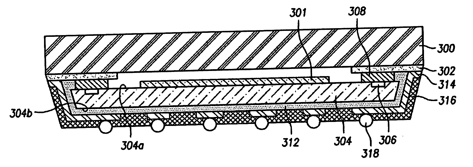
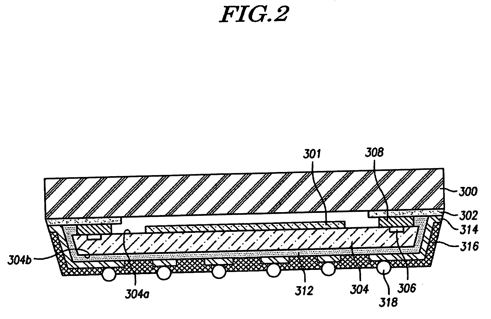
[0021]FIG. 2 is a cross-sectional view of an embodiment of an image sensor chip package according to the present invention. In the image sensor chip package as shown in FIG. 2, a first surface 304a of a chip 304 from a silicon wafer is provided with a light transmittance or sensing element 301 and chip pads 306. Chip 304 and / or chip pads 306 are electrically and physically attached to a glass substrate 300 with conductive material 308.
[0022] The glass substrate 300 is provided with electrode pads 302. The electrode pads 302 are connected to metal wiring pattern (or inter-surface connection) 314, which is placed along a second surface 304b of the chip 304. A protective film 312 is formed on the second surface 304b of the chip 304, and the metal wiring pattern 314 is generally formed on protective film 312. In addition, a solder-resist 316 covers an exposed portion of the metal wiring pattern 314 where it is not in contact with solder balls (or solder bumps) 318. An infrared filter m...
PUM
 Abstract
Description
Claims
Application Information
 - R&D
- Intellectual Property
- Life Sciences
- Materials
- Tech Scout
- Unparalleled Data Quality
- Higher Quality Content
- 60% Fewer Hallucinations
Browse by: Latest US Patents, China's latest patents, Technical Efficacy Thesaurus, Application Domain, Technology Topic, Popular Technical Reports.
© 2025 PatSnap. All rights reserved.Legal|Privacy policy|Modern Slavery Act Transparency Statement|Sitemap|About US| Contact US: help@patsnap.com