Semiconductor integrated circuit device which restricts an increase in the area of a chip, an increase in the number of lead terminals of a package, and can reduce parasitic inductance

a technology of integrated circuits and semiconductors, applied in semiconductor devices, semiconductor/solid-state device details, electrical devices, etc., can solve the problems of affecting the circuit properties of integrated circuit chips, becoming critical problems, and significantly deteriorating circuit properties, so as to reduce parasitic inductance, increase the chip area, and increase the number of lead terminals

Inactive Publication Date: 2006-03-02
SHARP KK
View PDF3 Cites 10 Cited by
  • Summary
  • Abstract
  • Description
  • Claims
  • Application Information

AI Technical Summary

Benefits of technology

[0013] The present invention is provided in order to solve the above described problems, and an object of the invention is to provide a semiconductor integrated circuit device which restricts an increase in the area of a chip and an increase in the number of lead terminals of the package, and in addition, can reduce the parasitic inductance in a simple configuration.
[0022] A semiconductor integrated circuit device of the present invention is provided with a first power supply line for commonly supplying one of a power supply voltage and a ground voltage to a first circuit and a second circuit which do not operate parallel to each other. Accordingly, the number of power supply lines can be reduced, and in addition, the number of terminals which are connected to the power supply lines can be reduced, so as to reduce the area of a chip.

Problems solved by technology

Meanwhile, it is known that bonding wires for making electrical connection between bonding pads and lead terminals of a semiconductor package have a parasitic inductance which greatly affects the circuit properties of the integrated circuit chip.
This has become a critical problem.
A problem arises in a grounded emitter amplifier circuit, which is cited as an example, where a bonding wire that is connected to a bonding pad to which a ground voltage GND is supplied has a parasitic inductance which occurs significantly degradation of the circuit properties, due to so-called emitter degeneration.
Here, emitter degeneration is a phenomenon where the existence of an impedance component between the emitter of a transistor and a grounded point causes degradation in the transconductance of the grounded emitter amplifier circuit due to negative feedback caused by the impedance, and thus, degradation in the power occurs.
In the configuration disclosed in the above described gazette, however, it is very difficult to determine the optimal capacitance value for reducing the impedance, and also, a problem arises, where the configuration becomes complex.
In particular, in a high frequency circuit, a bonding wire has a parasitic inductance, which greatly affects the circuit properties, and in the case where the range of utilized frequencies of an input signal, that is, the frequency band, is broad, a problem arises, where it is difficult to gain a sufficient effect in the above described configuration.
However, reduction in the area of a chip and reduction in the number of lead terminals of the package is generally desired in a semiconductor integrated circuit device, from the point of view of miniaturization and cost reduction, and the above described system has a problem where an increase in the area of a chip, together with an increase in the number of bonding pads and an increase in the number of lead terminals of the package, is possible.

Method used


Image

  • Semiconductor integrated circuit device which restricts an increase in the area of a chip, an increase in the number of lead terminals of a package, and can reduce parasitic inductance
  • Semiconductor integrated circuit device which restricts an increase in the area of a chip, an increase in the number of lead terminals of a package, and can reduce parasitic inductance
  • Semiconductor integrated circuit device which restricts an increase in the area of a chip, an increase in the number of lead terminals of a package, and can reduce parasitic inductance

Examples


first embodiment

[0031] In reference to FIG. 1, an integrated circuit chip TP according to a first embodiment of the present invention includes first to fourth circuit blocks 1 to 4, a number of bonding pads PD which are placed in the peripheral region of the circuit blocks, VDD lines V1 to V4, and GND lines G1, G3 and G4. First to fourth circuit blocks 1 to 4 are connected to respective corresponding VDD lines V1 to V4, so as to receive a supply of a power supply voltage VDD. In addition, first and second circuit blocks 1 and 2 are commonly connected to GND line G1, so as to receive a supply of a ground voltage GND from GND line G1. In addition, third and fourth circuit blocks 3 and 4 receive a supply of ground voltage GND from GND lines G3 and G4, respectively. In the present embodiment, the input / output lines to / from respective circuit blocks 1 to 4 are omitted. Here, the VDD lines and the GND lines are power supply lines for supplying power supply voltage VDD and ground voltage GND, respectively...

second embodiment

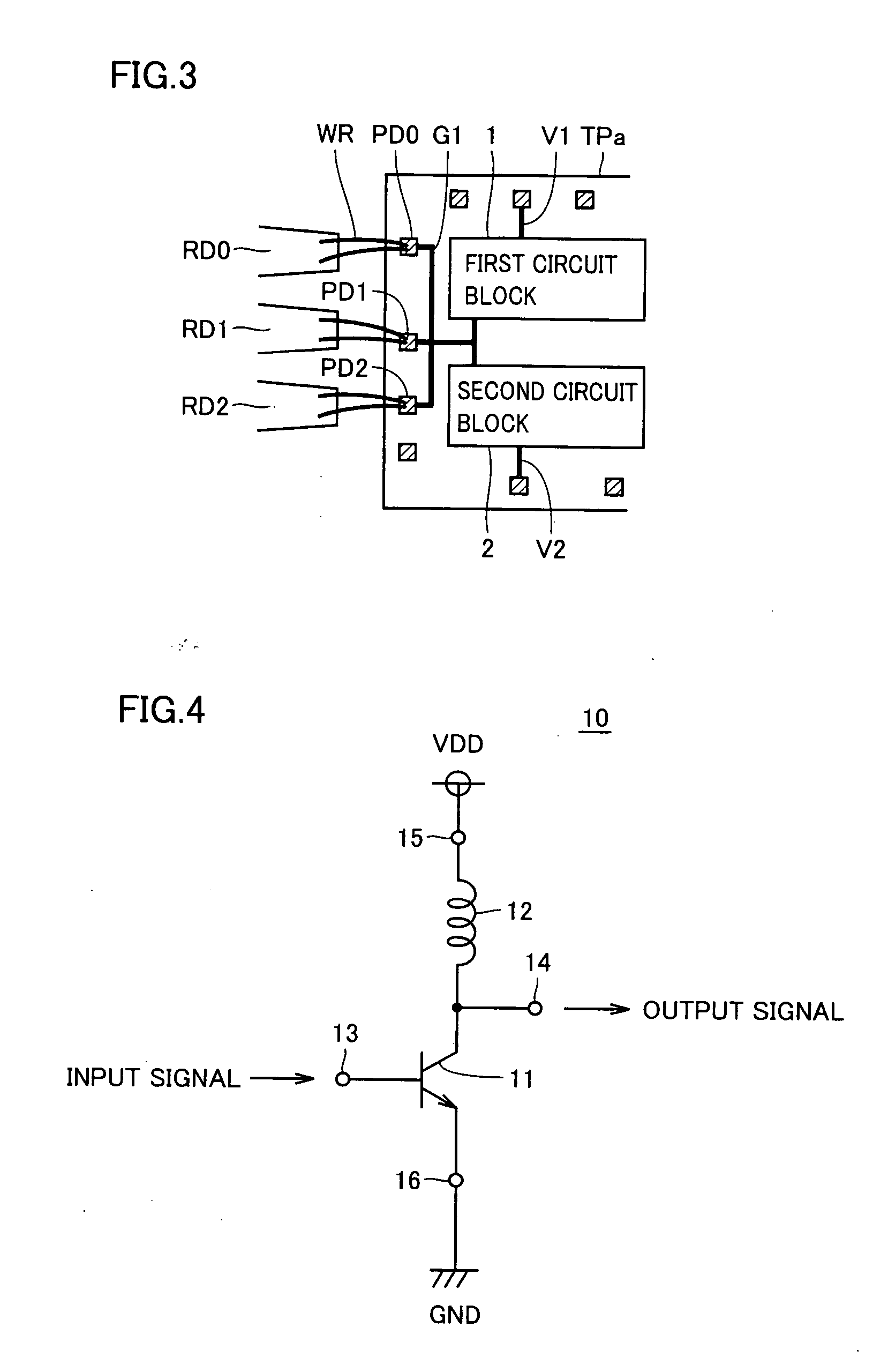
[0038] In reference to FIG. 2, an integrated circuit chip TPa according to a second embodiment of the present invention is different from integrated circuit chip TP according to the first embodiment of the present invention, in that GND line G1 is connected to three bonding pads PD0 to PD2. Other portions are the same as in integrated circuit chip TP of FIG. 1, and therefore, the detailed descriptions thereof are not repeated. Here, parts that are the same in the respective drawings are denoted by the same symbols.

[0039] In the chip configuration according to the second embodiment of the present invention, the above described GND line GI is shared by a number of circuit blocks, providing a state of connection to a number of bonding pads PD that are not being utilized, and therefore, it becomes possible to reduce the parasitic inductance, due to the connection of a plurality of bonding wires, while restricting an increase in the number of GND terminals as a whole.

[0040] Here, thoug...

fourth embodiment

[0045] In reference to FIG. 4, a grounded emitter amplifier circuit 10 according to a fourth embodiment of the present invention includes a bipolar transistor 11, a load inductor 12, an input terminal 13 for grounded emitter amplifier circuit 10, an output terminal 14 for grounded emitter amplifier circuit 10, a power supply terminal 15 that is connected to a VDD line, and a GND terminal 16 that is connected to a GND line.

[0046] Grounded emitter amplifier circuit 10 amplifies an input signal from input terminal 13 by a predetermined amplification ratio on the basis of load inductor 12 and bipolar transistor 11, and outputs the resulting signal to output terminal 14.

[0047] In the case where such a grounded emitter amplifier circuit 10 is provided as a first circuit block in FIGS. 1 to 3, for example, the impedance between the emitter and the ground of the grounded emitter amplifier circuit is reduced when GND terminal 16 is connected to the GND line, as in FIGS. 1 to 3. Accordingly...


PUM


Abstract

A semiconductor integrated circuit device according to the present invention has a configuration where a GND line is shared by a first circuit block and a second circuit block from among a number of circuit blocks provided on a semiconductor substrate, where the first circuit block and the second circuit block are in a state where they do not operate parallel to each other. In addition, one bonding pad and the GND line are electrically connected to each other. Accordingly, one GND terminal is provided for two circuit blocks, and therefore, it is possible to reduce the number of lead terminals.

Description

[0001] This nonprovisional application is based on Japanese Patent Application No. 2004-255950 filed with the Japan Patent Office on Sep. 2, 2004, the entire contents of which are hereby incorporated by reference. BACKGROUND OF THE INVENTION [0002] 1. Field of the Invention [0003] The present invention relates to a semiconductor integrated circuit device that includes circuits only one of which operates at a time, such as a transmission system circuit and a receiving system circuit of a high frequency communication device, and in particular, to a semiconductor integrated circuit device where electrical connection between an integrated circuit chip and a semiconductor package is made by means of bonding wires. [0004] 2. Description of the Background Art [0005] In general, an integrated circuit chip of a semiconductor circuit integrated device (hereinafter also simply referred to as chip) has a number of bonding pads on the upper surface thereof, and this number of bonding pads are al...

Claims


Application Information

Patent Timeline
Patent Type & Authority Applications(United States)
IPC IPC(8): H01L27/10H01L21/44
CPCH01L23/5286H01L2224/05554H01L24/49H01L2224/05599H01L2224/48091H01L2224/48245H01L2224/49111H01L2224/49112H01L2224/49171H01L2224/85399H01L2924/01004H01L2924/01005H01L2924/01033H01L2924/01046H01L2924/01082H01L2924/14H01L2924/19042H01L2924/19043H01L2924/30105H01L2924/30107H01L2924/3011H01L24/06H01L2924/1305H01L24/48H01L2224/48247H01L2924/00014H01L2924/01006H01L2924/01068H01L2224/45099H01L2924/00H01L2224/023H01L2924/0001
Inventor SAKURAI, SHOJI
Owner SHARP KK
Why Eureka
Try Eureka