IP-based LSI design system and design method
a design system and lsi technology, applied in the field of so-called, can solve the problems of increasing design man-hours, low design efficiency, and considerable design man-hours for new designs, and achieve the effect of reducing design man-hours and improving design efficiency in ip-based lsi design
- Summary
- Abstract
- Description
- Claims
- Application Information
AI Technical Summary
Benefits of technology
Problems solved by technology
Method used
Image

Examples
first embodiment
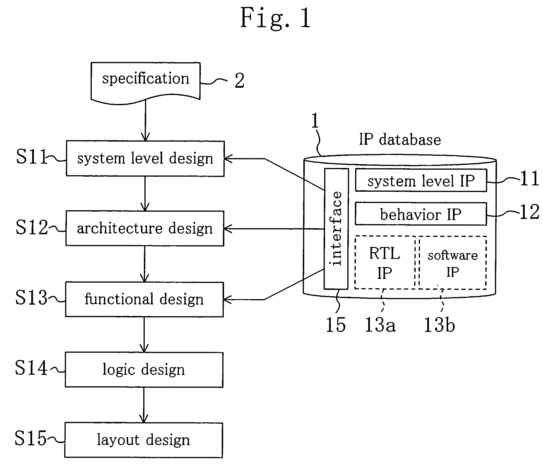
[0045]FIG. 1 is a conceptual diagram illustrating IP-based LSI design. As shown in FIG. 1, IP-based LSI design is carried out hierarchically in the order of system level design S11, architecture design S12, functional design S13, logic design S14 and layout design S15. In the system level design S11, the architecture design S12 and the functional design S13, which are the upstream processes, an IP database 1 is utilized, which stores so-called IPs used for the LSI design.
[0046] The IP database 1 stores system level IPs 11 having information of the system level, behavior IPs 12 having information of the architecture level and RTL IPs 13a or software IPs 13b having information of the functional level, each of which is associated with a corresponding IP. In the system level design S11, the system level IP 11 is reused. In the architecture design S12, the behavior IP 12 corresponding to the reused system level IP 11 is retrieved via an interface 15, whereas in the functional design S13...
second embodiment
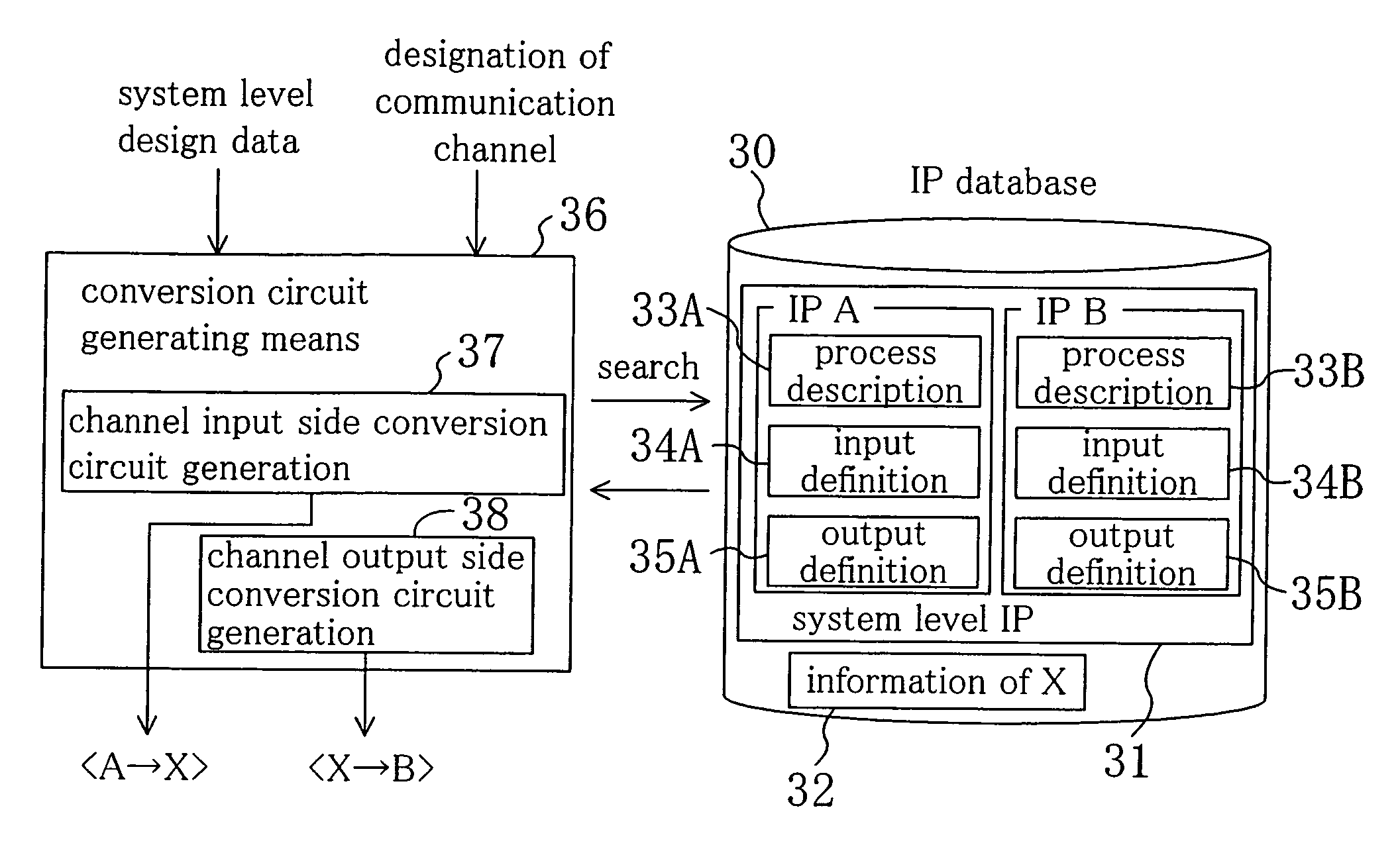
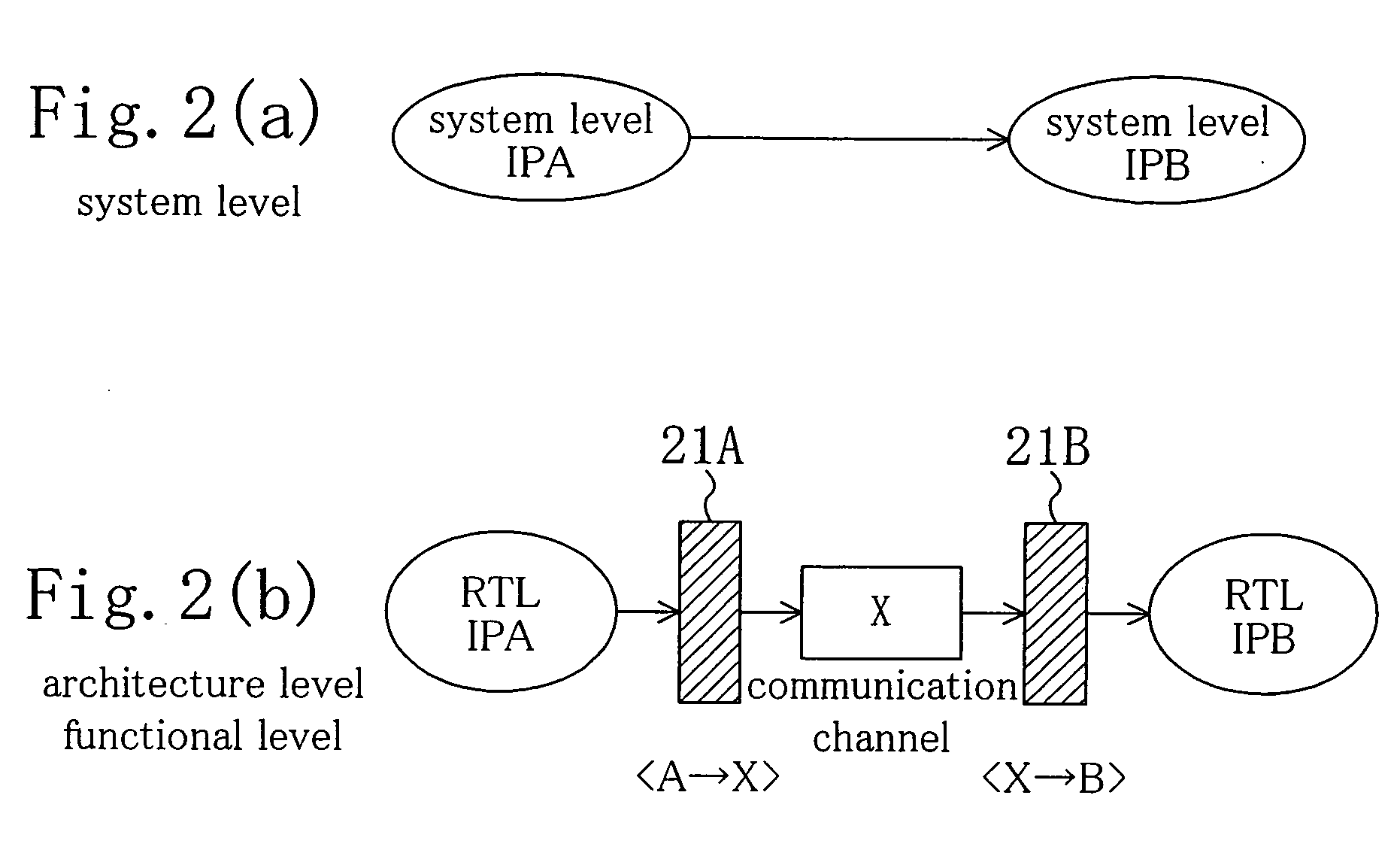
[0061] When an applicable IP is selected by searching the IP database in IP-based LSI design, it is very rare that the selected IP can be used as is for the LSI to be newly designed. Actually, it seems that, in most cases, the selected IP is inappropriate because of specification problems, or even when it is applicable, revisions and verifications are required. This problem increases the design man-hours and hinders realization of the efficient LSI design.
[0062] With a so-called target-driven reuse and design method of allocating components in accordance with requirement specifications, this problems is inevitable. Therefore, the inventors of the present invention propose a so-called IP-DB-driven reuse and design method. This method classifies input data into structural elements for which the possibility is high that there are existing design assets (IPs), so that the existing IPs can be used efficiently.
[0063]FIG. 10 is a diagram showing a configuration of an IP-based LSI design ...
third embodiment
[0075]FIG. 16 is a diagram illustrating the configuration of an IP-based LSI design system according to the third embodiment of the present invention. In this embodiment, a low-power system LSI (with reduced power consumption) can be realized by utilizing IPs efficiently in the top-down design of the system LSI.
[0076] First, in the system level design, a function definition 91 according to a system level IP is obtained with respect to the LSI to be designed. Next, in an architecture generation step S31, design data 92 of the architecture level are generated from the function definition 91 according to the system level IP. Then, in an operation analysis step S32, operation analysis of the LSI to be designed is carried out using these design data 92 of the architecture level, a command 93 and an operation pattern definition 94 that defines the operation of the system LSI.
[0077]FIG. 17 is a diagram showing an example of the operation analysis results. In FIG. 17, it is necessary to s...
PUM
 Abstract
Description
Claims
Application Information
 - R&D
- Intellectual Property
- Life Sciences
- Materials
- Tech Scout
- Unparalleled Data Quality
- Higher Quality Content
- 60% Fewer Hallucinations
Browse by: Latest US Patents, China's latest patents, Technical Efficacy Thesaurus, Application Domain, Technology Topic, Popular Technical Reports.
© 2025 PatSnap. All rights reserved.Legal|Privacy policy|Modern Slavery Act Transparency Statement|Sitemap|About US| Contact US: help@patsnap.com