Etching method, a method of forming a trench isolation structure, a semiconductor substrate and a semiconductor apparatus

a trench isolation and etching method technology, applied in the direction of semiconductor devices, cleaning processes and apparatus, semiconductor devices, etc., can solve the problems of incomplete device isolation, large device isolation region of locos method, and inability to fully isolate adjacent devices, etc., to achieve high reliability

Inactive Publication Date: 2006-02-16
SEIKO EPSON CORP +1
View PDF5 Cites 2 Cited by
  • Summary
  • Abstract
  • Description
  • Claims
  • Application Information

AI Technical Summary

Benefits of technology

[0064] This makes it possible to obtain a...

Problems solved by technology

However, in the case where an oxide film having a minute pattern is formed using the LOCOS method, device isolation becomes incomplete because oxidation in a thickness direction does not proceed sufficiently.
For this reason, the miniaturization of the device isolation region in the LOCOS method has its own limitation.
The dishing occurs because polishing does not proceed evenly between a narrow portion and a wide portion of the device isolation pattern due to a difference between the etching rates therefor.
Since the SiO2 film 600 is excessively polished at a relatively wide device isolation region in the dishing, isolation between the adjacent devices separated with such a...

Method used


Image

  • Etching method, a method of forming a trench isolation structure, a semiconductor substrate and a semiconductor apparatus
  • Etching method, a method of forming a trench isolation structure, a semiconductor substrate and a semiconductor apparatus
  • Etching method, a method of forming a trench isolation structure, a semiconductor substrate and a semiconductor apparatus

Examples


example

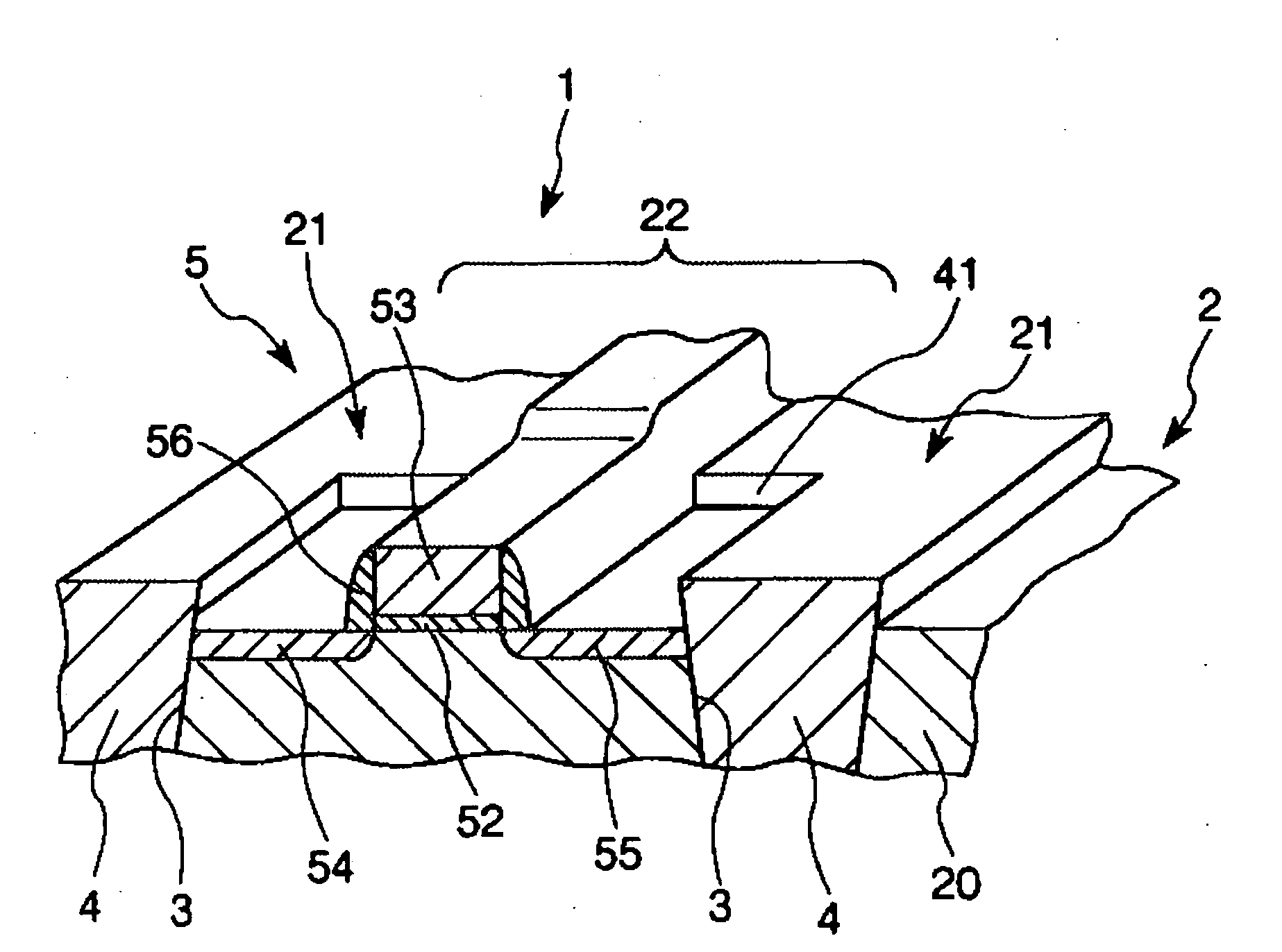
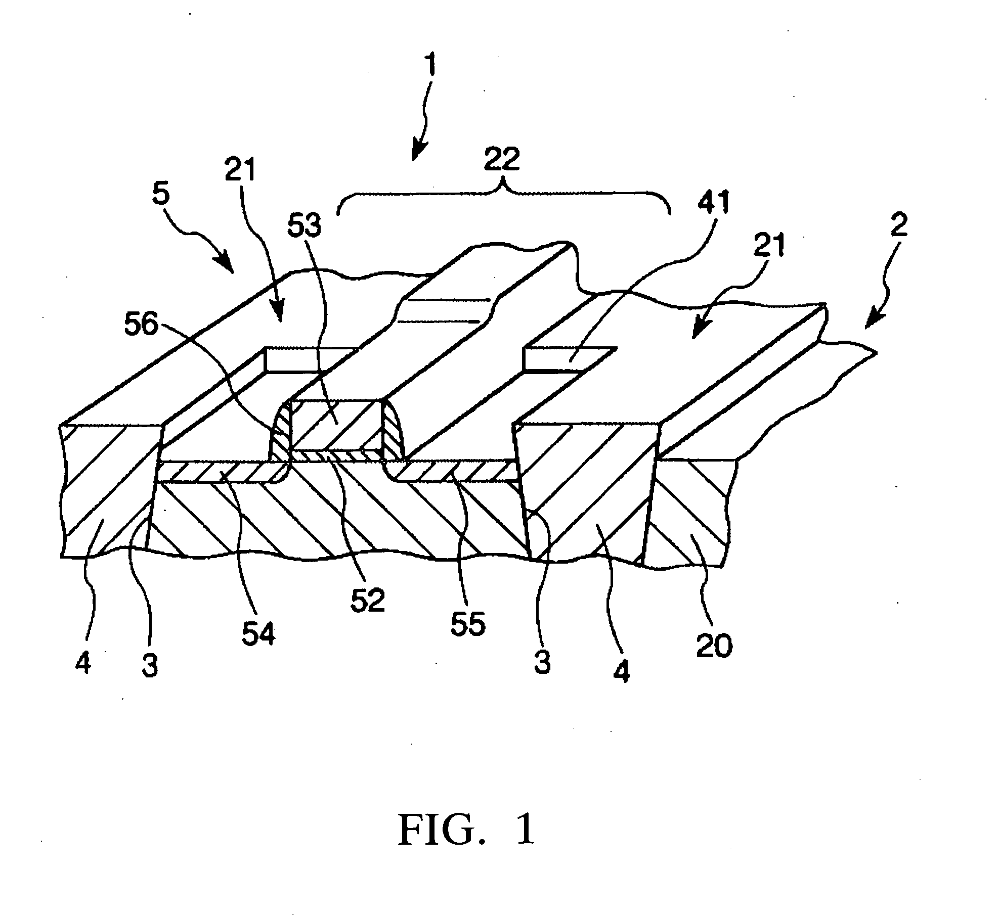
[0160] First, a p type single crystal silicon substrate having the orientation of (100) (hereinafter, referred to simply as “silicon substrate”) was prepared.

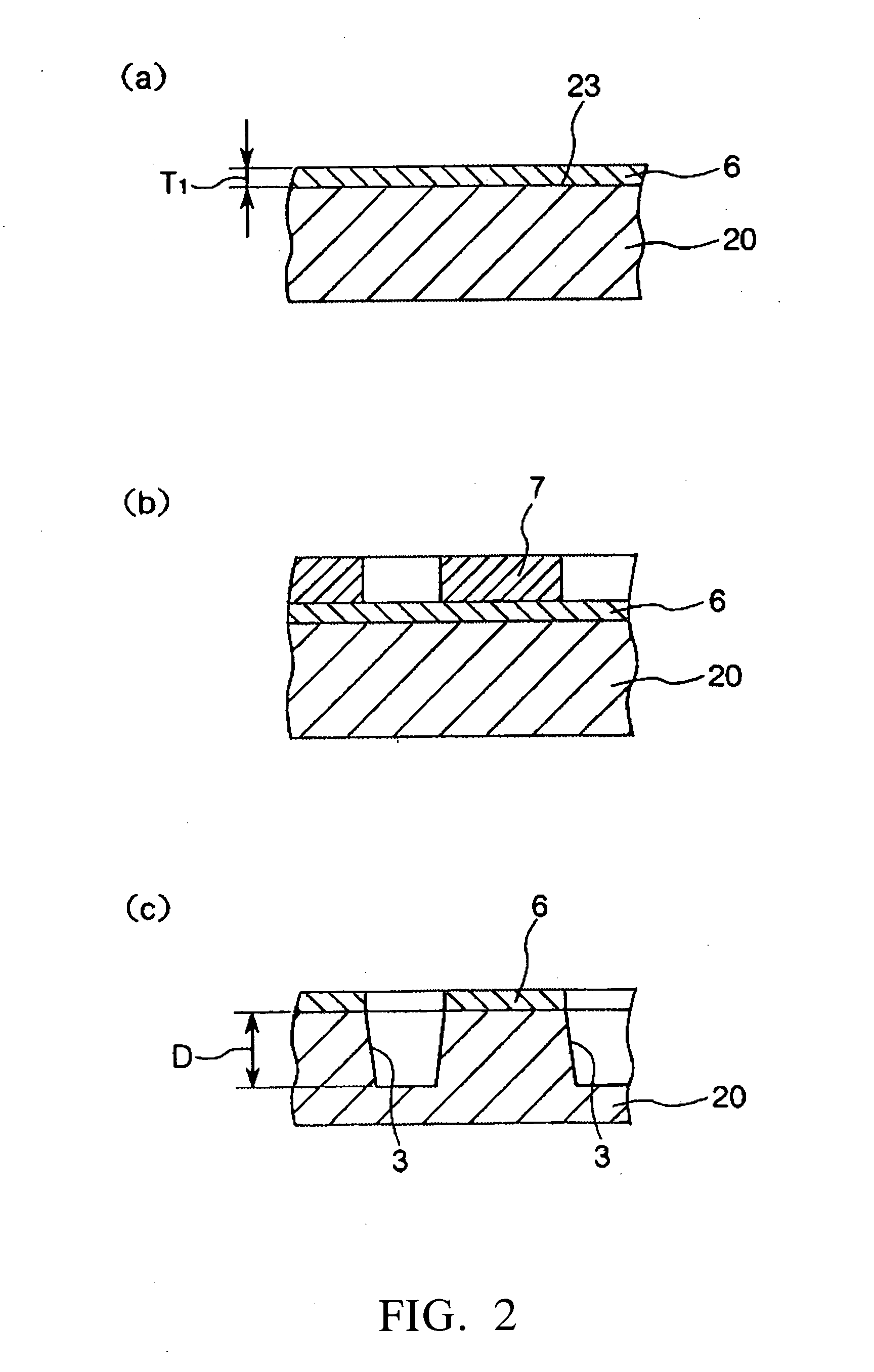
[0161] Next, the silicon substrate was subjected to a thermal oxidation process in which the silicon substrate was heated at 900° C. for 20 minutes under the atmosphere including O2 and N2. Thus, a SiO2 film (that is, pad oxide film) having an average thickness of 10 nm was formed on the surface of the silicon substrate.

[0162] Next, a resist layer shaped of having openings respectively corresponding to device forming regions was formed on the SiO2 film by means of a photolithography method. The SiO2 film and silicon substrate were eliminated by means of a reactive ion etching method using the resist layer as a mask. Thus, trenches each having a depth of 400 nm from the surface of the silicon substrate were formed.

[0163] Next, after eliminating the resist layer, an insulating material (SiO2) was supplied onto the silicon subs...


PUM

PropertyMeasurementUnit
Temperatureaaaaaaaaaa
Fractionaaaaaaaaaa
Percent by massaaaaaaaaaa

Abstract

An etching method of subjecting a base material to an etching process using an etching agent containing hydrogen fluoride and ozone is disclosed. The base material has a first region constituted from silicon as a main material and a second region constituted from SiO2 as a main material. The etching method includes the steps of: preparing the base material; and supplying the etching agent onto the base material to form a step between the first and second regions using a feature that an etching rate of silicon by the etching agent is higher than an etching rate of SiO2 by the etching agent, so that the height of the surface of the first region is lower than the height of the surface of the second region.

Description

CROSS-REFERENCE TO RELATED APPLICATION [0001] This application claims priority to Japanese Patent Application No. 2004-236181 filed Aug. 13, 2004, which is hereby expressly incorporated by reference herein in its entirety. FIELD OF THE INVENTION [0002] The present invention relates to an etching method, a method of forming a trench isolation structure, a semiconductor substrate and a semiconductor apparatus. BACKGROUND OF THE INVENTION [0003] A demand for high density and high integration of semiconductor devices in a semiconductor apparatus tends to heighten. In order to respond such a demand, miniaturization of a semiconductor device itself, and miniaturization of a device isolation region for isolating adjacent semiconductor devices tend to become increasingly important. Heretofore, as a method of forming a device isolation region, a LOCOS (Local Oxidation of Silicon) method in which an oxide film to become a device isolation region is formed has been generally utilized. [0004] H...

Claims


Application Information

Patent Timeline
IPC IPC(8): H01L29/00H01L21/76
CPCH01L21/30604H01L21/31055H01L29/66575H01L21/76224H01L21/823481H01L21/31111H01L21/306H01L21/76
Inventor MATSUO, HIROYUKINAKAJIMA, TOSHIKIMIYAZAKI, KUNIHIRO
Owner SEIKO EPSON CORP
Why Eureka
Try Eureka