Electrostatic discharge protection device

a protection device and electrostatic discharge technology, applied in semiconductor devices, semiconductor/solid-state device details, diodes, etc., can solve the problems of ic being punched through or burned out suddenly, generating extra noises that affect the total ic noise figures, and esd damage could become a serious problem, so as to reduce the problem of substrate noise

Inactive Publication Date: 2006-02-09
CHEN SHIAO SHIEN
View PDF2 Cites 5 Cited by
  • Summary
  • Abstract
  • Description
  • Claims
  • Application Information

AI Technical Summary

Benefits of technology

[0034] Accordingly, since the ESD component is provided for the ESD clamp circuit of the ESD protection circuit of the present invention, the parasitic capacitance of the ESD clamp circuit is much less than that of the conventional diode string. In addition, since the ESD component dose not constructed by the substrate of the ESD clamp circuit of the ESD protection circuit, the problem of the substrate noise may be reduced.

Problems solved by technology

However, as the area and the tolerance of the integrated circuits (IC) reduce, the damage caused by the electrostatic discharge (ESD) could become a serious problem.
Therefore, when the integrated circuit (IC) is damaged by the ESD, the IC might get punched through or burned out suddenly.
In addition, the ESD protection circuit also introduce noise coupling due to parasitic capacitance and will generate extra noises that will affect total IC noise figures.
Therefore, the conventional RF ESD protection circuit 100 shown in FIG. 1A and FIG. 1B has the disadvantages that the parasitic capacitance of the diode string 110 is large.
Thus, the performance of the RF IC 102 is degraded or even failed.
Therefore, the performance of the RF IC 102 is seriously degraded by the substrate noise.

Method used


Image

  • Electrostatic discharge protection device
  • Electrostatic discharge protection device
  • Electrostatic discharge protection device

Examples


Embodiment Construction

[0050] The present invention now will be described more fully hereinafter with reference to the accompanying drawings, in which preferred embodiments of the invention are shown. This invention may, however, be embodied in many different forms and should not be construed as limited to the embodiments set forth herein; rather, these embodiments are provided so that this disclosure will be thorough and complete, and will fully convey the scope of the invention to those skilled in the art. Like numbers refer to like elements throughout.

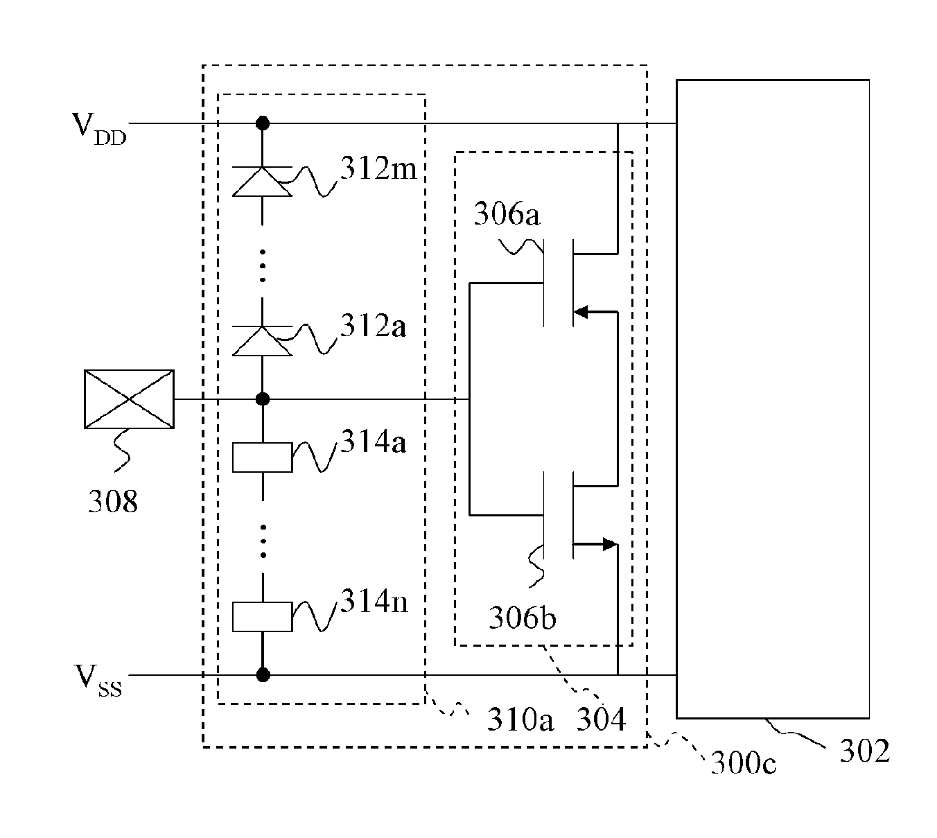
[0051]FIG. 3A is a schematic circuit diagram of an ESD protection circuit according to one embodiment of the present invention. Referring to FIG. 3A, an ESD protection circuit 300a comprises, for example but not limited to, an ESD clamp circuit 310a connected to an I / O pad 308 and connected between voltages VDD and VSS of IC 302. In one embodiment of the present invention, the voltages VDD and VSS represent a high voltage and a low voltage or vice versa....


PUM


Abstract

An electrostatic discharge (ESD) protection device including an ESD clamp circuit is provided. The ESD clamp circuit includes at least a diode connected in series between a first voltage and a pad, and at least an ESD component connected in series between a second voltage and a pad. Each of the at least an ESD component comprises a deep N-well region formed in a P-type substrate, a triple P-well formed in the deep N-well region, and a highly doped N-type (N+) region and a highly doped P-type (P+) region formed in the triple P-well region.

Description

CROSS-REFERENCE TO RELATED APPLICATION [0001] This application is a divisional of a prior application Ser. No. 09 / 990,392, filed Nov. 20, 2001, now pending.BACKGROUND OF THE INVENTION [0002] 1. Field of the Invention [0003] The present invention is related to an electrostatic discharge (ESD) protection device. More particularly, the present invention relates to an ESD protection device for bypassing an ESD current with low-capacitance and low substrate noise. [0004] 2. Description of Related Art [0005] As the semiconductor technology advances, the integration of the semiconductor devices are enhanced by, for example, reducing the line width and increasing the stacked layers of the semiconductor device. However, as the area and the tolerance of the integrated circuits (IC) reduce, the damage caused by the electrostatic discharge (ESD) could become a serious problem. Conventionally, the waveform of the electrostatic discharge (ESD) has the properties of short rise time (e.g., generall...

Claims


Application Information

Patent Timeline
Patent Type & Authority Applications(United States)
IPC IPC(8): H01L23/62
CPCH01L27/0255
Inventor CHEN, SHIAO-SHIEN
Owner CHEN SHIAO SHIEN
Why Eureka
Try Eureka