Ion implantation apparatus and method for implanting ions by using the same

Inactive Publication Date: 2006-02-02
SK HYNIX INC
View PDF5 Cites 6 Cited by
  • Summary
  • Abstract
  • Description
  • Claims
  • Application Information

AI Technical Summary

Problems solved by technology

However, in this transistor formation method the transistors are not uniformly formed on the entire regions of a wafer.
For instance, a mask process and an etching process are required to form the gate spacers, and during the gate spacer formation, it is difficult to obtain uniform lengths of the gate spacers.
It is also difficult to obtain uniformity in the gate structures with the stacked layers for each application of a gate structure process.
As shown, the dose of implanted ions is higher at the edges than in the center; accordingly, the dose of implanted ions is not uniform on the wafer.
This nonuniform scattering results from a threshold voltage of a transistor and other electric parameters differently set between the transistors because of various factors impeding uniformity of the wafer.
However, this approach of ion implantation causes a much higher transistor threshold voltage at the edges of the wafer because it is difficult to implant ion impurities with different required concentrations throughout the single wafer.
That is, although it is possible to adjust the transistor parameters by controlling the ion implantation recipe, it is difficult to improve transistor characteristics at the desired region.

Method used


Image

  • Ion implantation apparatus and method for implanting ions by using the same
  • Ion implantation apparatus and method for implanting ions by using the same
  • Ion implantation apparatus and method for implanting ions by using the same

Examples


Embodiment Construction

[0032] An ion implanter for uniformity of transistor parameters and an ion implantation method using the same in accordance with a preferred embodiment of the present invention are described in detail with reference to the accompanying drawings.

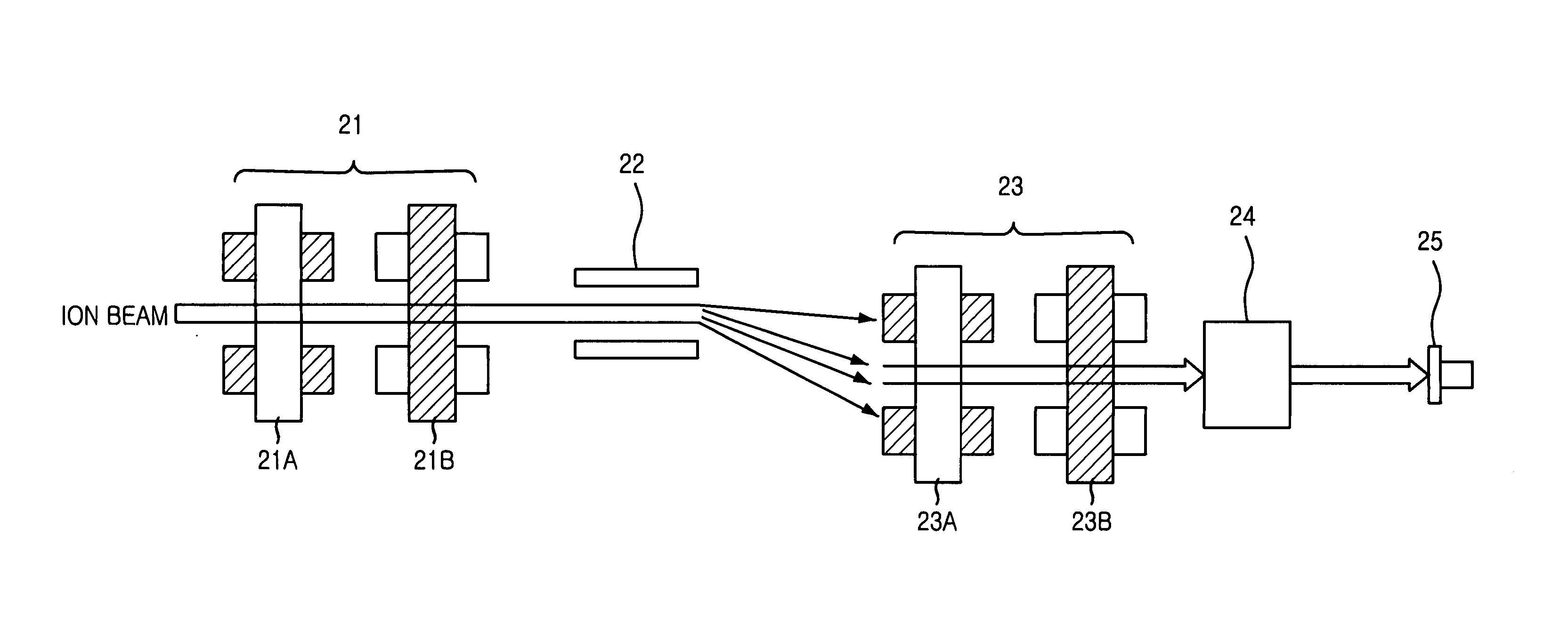
[0033]FIG. 3 shows an ion implanter in accordance with the present invention.

[0034] The ion implanter includes a first quadrupole magnet assembly 21, an X / Y-scanner 22, a second quadrupole magnet assembly 23, a beam parallelizer 24 and a wafer 25.

[0035] First quadrupole magnet assembly 21 helps both to focus an ion beam transmitted from an ion beam source and to generate magnetic fields at an interspatial pole between four magnetic poles. Particularly, first quadrupole magnet assembly 21 includes a first magnet subassembly 21A and a second magnet subassembly 21B, each having two South (S) poles S1 and S2 and two North (N) poles N1 and N2.

[0036] X / Y-scanner 22 helps to rapidly deflect the ion beam passed through first quadrupole magnet ass...


PUM


Abstract

Disclosed are an ion implantation apparatus and a method for implanting ions by using the same. The ion implanter for implanting ions into a wafer, includes: a first quadrupole magnet assembly for focusing an ion beam transmitted from an ion beam source; a scanner for deflecting the transmitted ion beam in the directions of an X-axis and an Y-axis; a second quadrupole magnet assembly for converging and diverging the ion beam passing through the scanner in the directions of the X- and Y-axes; and a beam parallelizer for rotating the ion beam in synchronization with the second quadrupole magnet assembly, thereby implanting the ion beam into the wafer.

Description

CROSS-REFERENCES TO RELATED APPLICATIONS [0001] NOT APPLICABLE STATEMENT AS TO RIGHTS TO INVENTIONS MADE UNDER FEDERALLY SPONSORED RESEARCH OR DEVELOPMENT [0002] NOT APPLICABLE REFERENCE TO A “SEQUENCE LISTING,” A TABLE, OR A COMPUTER PROGRAM LISTING APPENDIX SUBMITTED ON A COMPACT DISK. [0003] NOT APPLICABLE BACKGROUND OF THE INVENTION [0004] 1. Field of the Invention [0005] The present invention relates to a semiconductor processing technology; and more particularly, to an ion implanter to improve uniformity of transistor parameters and an implantation method using the same. [0006] 2. Description of Related Arts [0007] Generally, a transistor formation method includes several steps. First, a gate structure is formed on a substrate, and a gate spacer is formed on both sidewalls of the structure. Afterward, an ion-implantation process for adjusting a threshold voltage is applied to predetermined regions of the substrate disposed beneath the gate structure and the spacer and then, an...

Claims


Application Information

Patent Timeline
IPC IPC(8): H01J37/08H01J37/147H01J37/317H01L21/265
CPCH01J37/147H01J2237/04922H01J37/3171H01L21/265
Inventor ROUH, KYOUNG-BONGJIN, SEUNG-WOOLEE, MIN-YONG
Owner SK HYNIX INC
Why Eureka
Try Eureka