Method for fabricating a mask ROM
- Summary
- Abstract
- Description
- Claims
- Application Information
AI Technical Summary
Benefits of technology
Problems solved by technology
Method used
Image

Examples
Embodiment Construction
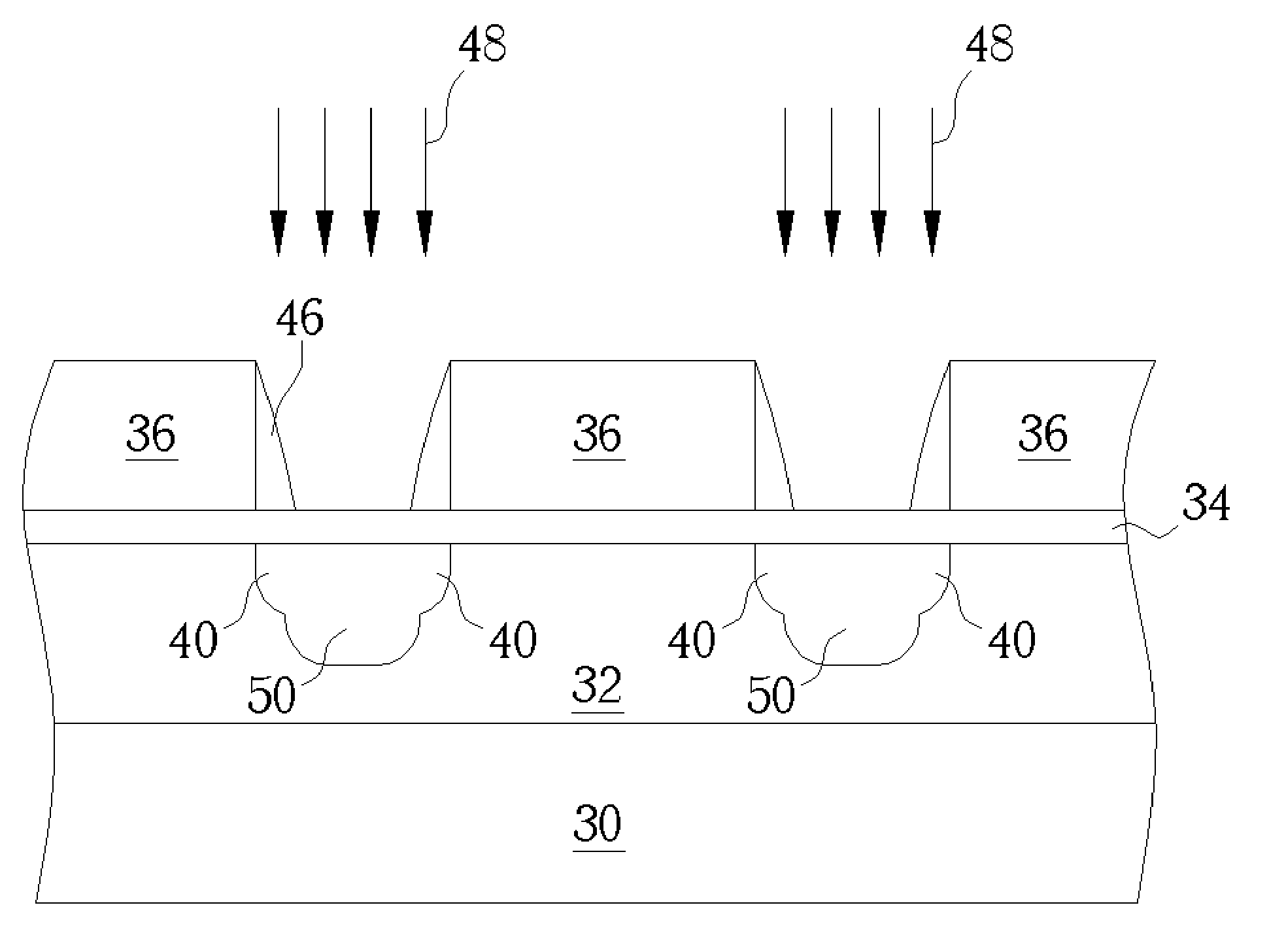
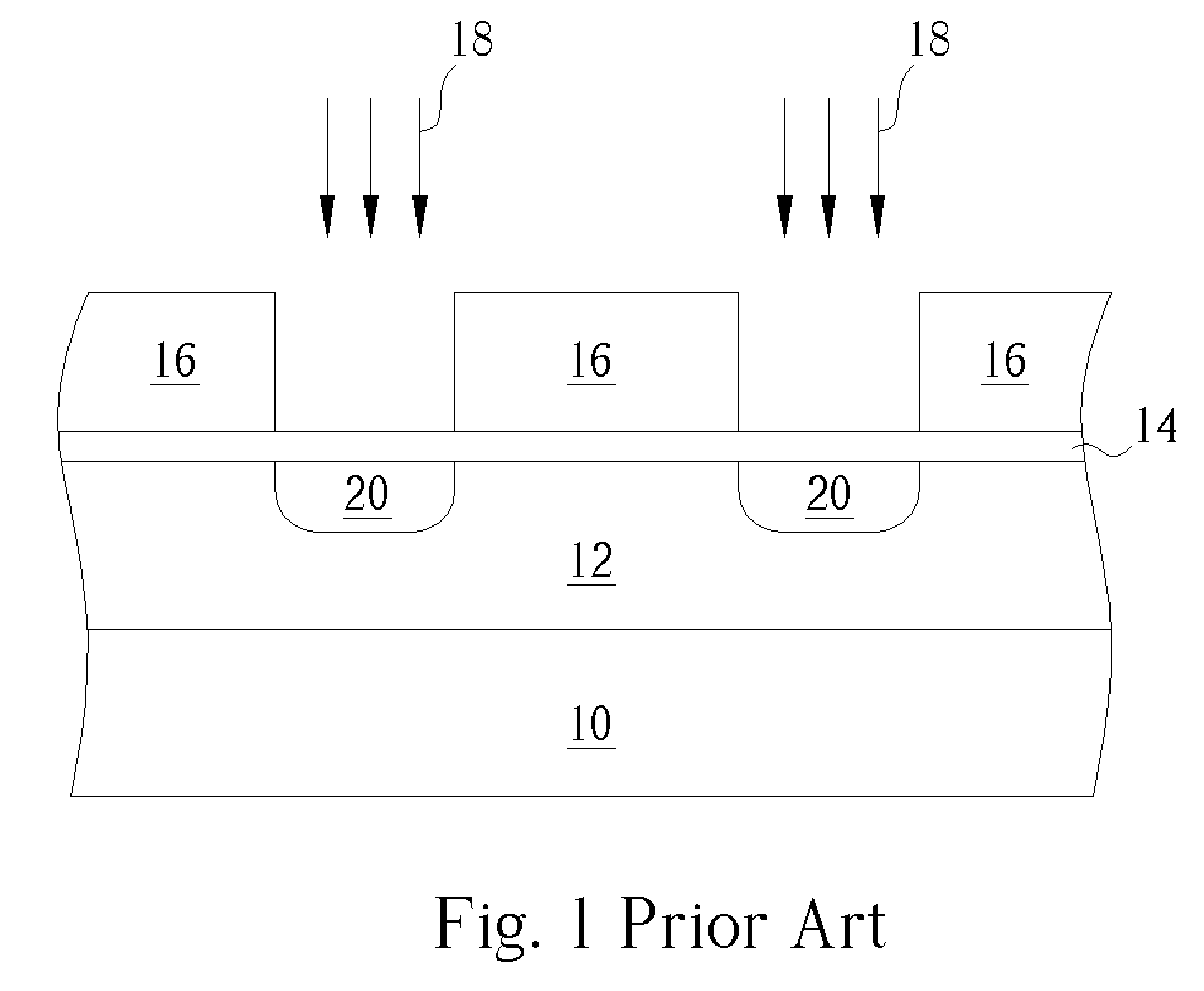
[0015]FIG. 3 to FIG. 9 are schematic diagrams for fabricating buried bit lines of the mask ROM according to one preferred embodiment of the present invention. Please refer to FIG. 3. A semiconductor substrate 30 comprising a P-type well 32 is provided. The surface of the semiconductor substrate 30 is thermally oxidized to form a pad oxide layer 34 with a thickness normally between 125 and 250 Å. A photoresist layer (not shown) is coated on the pad oxide layer 34 and patterned as in the art to form a photoresist pattern 36.
[0016] Please refer to FIG. 4, a first ion implantation process 38 is performed to form a first N-type or P-type doped region 40. The first doped region 40 is a lightly doped drain (LDD) region within the P-type well 32 not covered by the photoresist pattern 36.
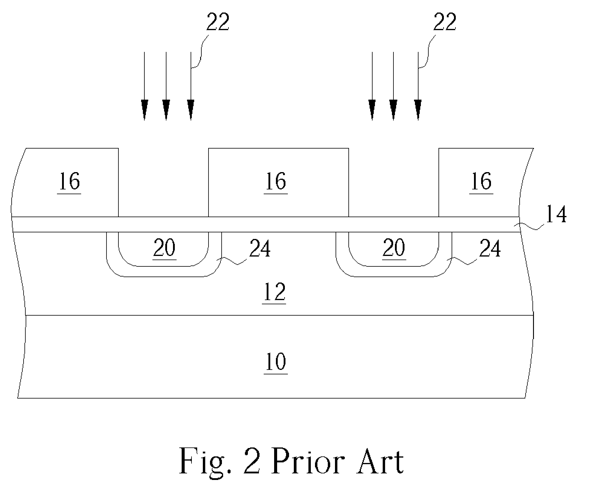
[0017] After forming the LDD region 40, as shown in FIG. 5, a hot treatment process 42 is performed to harden the photoresist pattern 36. Typically, the hot treatment process 42 is an UV curing process or ...
PUM
 Abstract
Description
Claims
Application Information
 - R&D
- Intellectual Property
- Life Sciences
- Materials
- Tech Scout
- Unparalleled Data Quality
- Higher Quality Content
- 60% Fewer Hallucinations
Browse by: Latest US Patents, China's latest patents, Technical Efficacy Thesaurus, Application Domain, Technology Topic, Popular Technical Reports.
© 2025 PatSnap. All rights reserved.Legal|Privacy policy|Modern Slavery Act Transparency Statement|Sitemap|About US| Contact US: help@patsnap.com