Radio frequency switching circuit

Inactive Publication Date: 2006-01-12
PANASONIC CORP
View PDF2 Cites 53 Cited by
  • Summary
  • Abstract
  • Description
  • Claims
  • Application Information

AI Technical Summary

Benefits of technology

[0023] The present invention provides an RF switching circuit which can eliminate the need for a directional coupler by using the power of a small transmitted signal leaking to the gate terminal of an FET constituting a transmission-side FET switching circuit, and is advantageous to miniaturization and low power consumption obtained by reducing a passage loss.
[0040] With this configuration, by eliminating the need for a directional coupler, it is possible to eliminate a passage loss occurring on a transmitted signal due to the directional coupler, thereby reducing the power consumption of the RF amplifier. When a main transmitter circuit including the RF amplifier and the RF switching circuit is entirely formed on a semiconductor substrate, the circuit is simplified by eliminating the need for a directional coupler, thereby greatly reducing a chip size and cost. Further, since a long strip line is not necessary on an integrated semiconductor substrate, it is possible to eliminate unnecessary electromagnetic coupling to other wires or elements, thereby preventing degradation of property and abnormal oscillation.

Problems solved by technology

However, the conventional art using the directional coupler 3 has the following problems:
1) Transmitted power has a passage loss due to the directional coupler 3 and the lost power has to be offset by an extra output of the RF amplifier for transmission, thereby increasing the current consumption of the RF amplifier for transmission.
2) When the function of the directional coupler 3 is formed on the substrate of a semiconductor integrated circuit together with the RF amplifier and the RF switching circuit, a long strip line is necessary on the substrate of the integrated circuit and occupies a large area, thereby increasing a chip size and cost.
3) Since the long strip line is present on the substrate of the integrated circuit, unnecessary electromagnetic coupling to other wires or elements appears, so that property degradation and abnormal oscillation may occur.

Method used


Image

  • Radio frequency switching circuit
  • Radio frequency switching circuit
  • Radio frequency switching circuit

Examples


embodiment 1

[0055] FIGS. 1 to 3 show Embodiment 1 of the present invention.

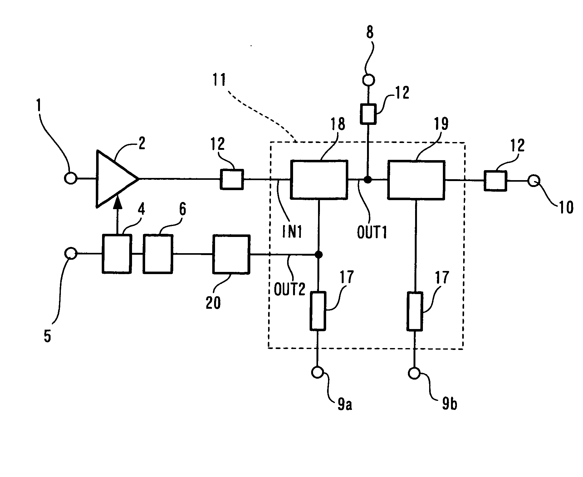
[0056] An RF switching circuit 11 shown in FIG. 1 comprises a transmission-side FET switching circuit 18, a reception-side FET switching circuit 19, an antenna-side input / output terminal 8, a received signal output terminal 10, transmit / receive switching control terminals 9a and 9b, control terminal protection elements 17, a DC signal component cut-off element 12, and a radio frequency signal passage element (hereinafter, referred to as an RF passage element) 20 serving as a coupling part allowing only the passage of a radio frequency signal component. A transmitted signal input terminal 1, an RF amplifier 2, a gain control circuit 4, a reference voltage input terminal 5, and a detector circuit 6 are provided in the previous stage of the RF switching circuit 11.

[0057] In the present embodiment, reference numeral IN1 denotes a first input where radio frequency output is inputted from the RF amplifier 2, reference numera...

embodiment 2

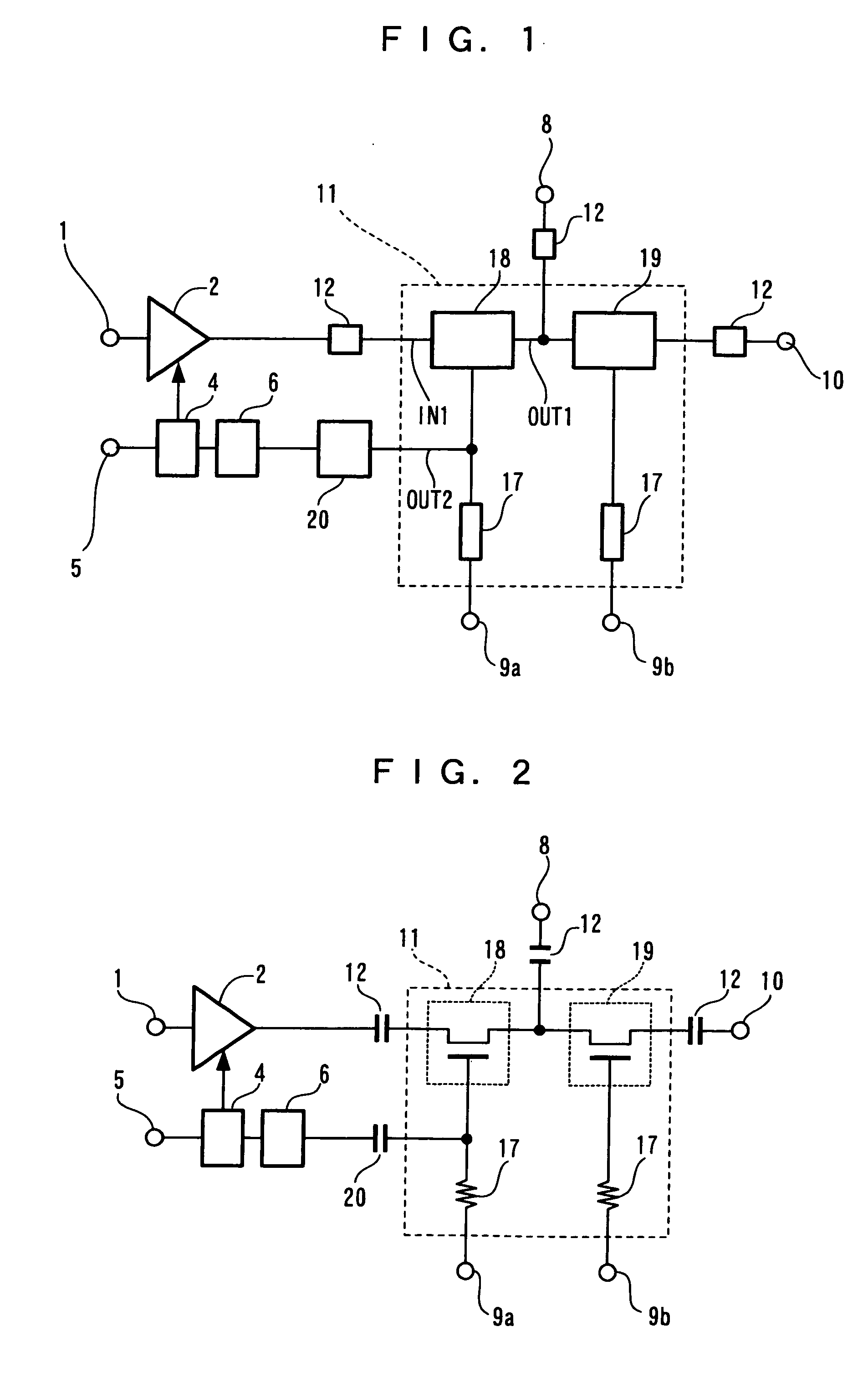
[0086]FIGS. 4 and 5 show Embodiment 2 of the present invention.

[0087] In FIGS. 1 and 2, only the transmission-side FET switching circuit 18 constitutes an FET switching circuit interposed between the first input fed with radio frequency output from the RF amplifier 2 and the antenna-side input / output terminal 8 for supplying radio frequency output to the subsequent stage of the radio frequency output. In Embodiment 2, as shown in FIG. 4, an FET switching circuit is constituted of a transmission-side through FET circuit 13 and a transmission-side shunt FET circuit 14.

[0088] The reception-side FET switching circuit 19 of FIGS. 1 and 2 is equivalent to a so-called SPDT RF switching circuit constituted of a reception-side through FET switching circuit 15 and a reception-side shunt FET switching circuit 16. In the RF switching circuit, a radio frequency transmitted signal leaking to the transmit / receive switching terminal of the transmission-side through FET circuit 13 is outputted to ...

embodiment 3

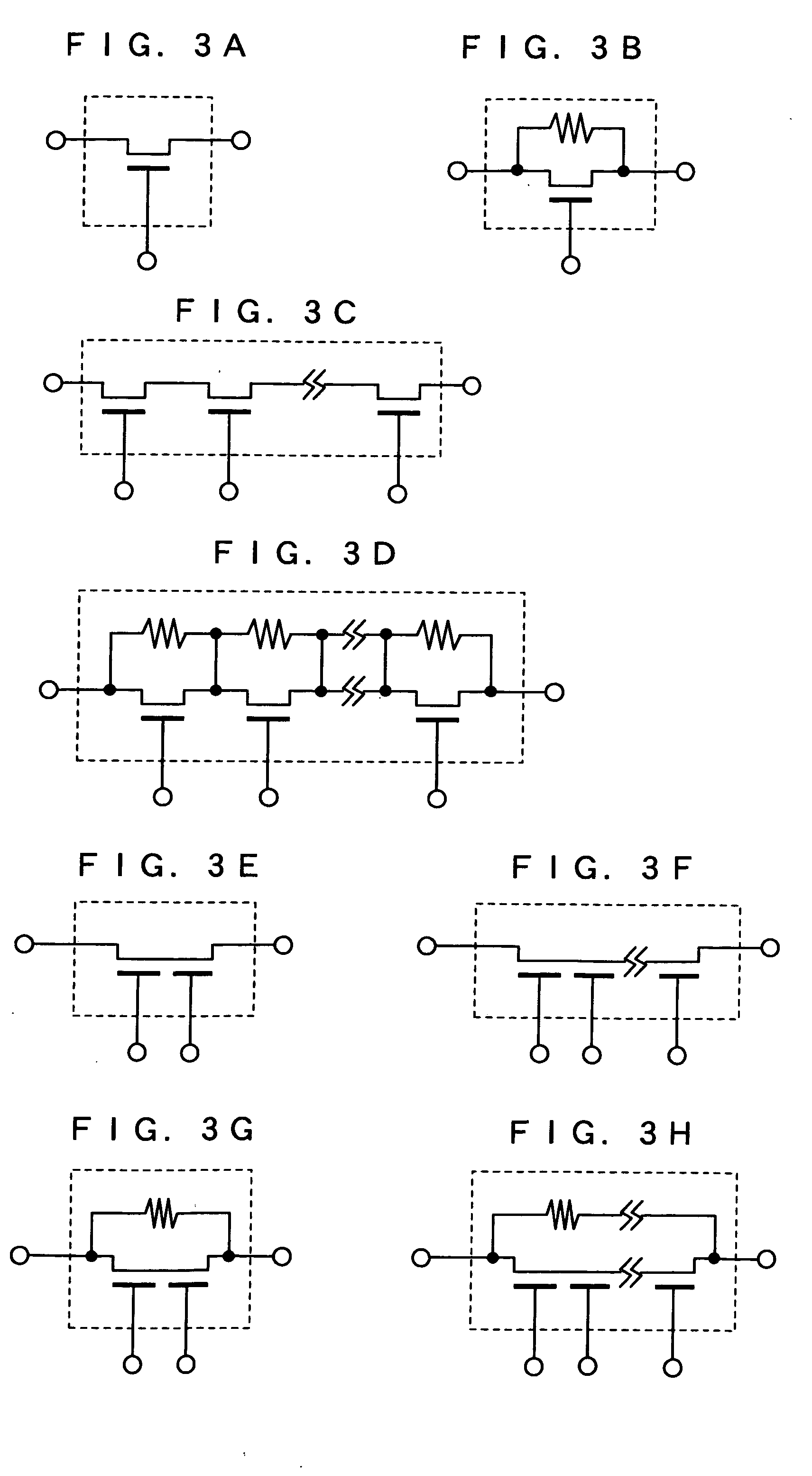
[0098] FIGS. 6 to 9 show Embodiment 3 of the present invention.

[0099] In FIG. 4, the main part of the RF switching circuit 11 is constituted of the transmission-side through FET circuit 13 and transmission-side shunt FET circuit 14 and the reception-side through FET circuit 15 and reception-side shunt FET circuit 16. In an RF switching circuit shown in FIG. 6, a transmission-side shunt FET circuit 14 is not absent and a reception-side through FET circuit 15 is constituted of a multistage FET where the source / drain terminals of two or more FETs are connected in series as shown in FIGS. 7 and 8.


PUM


Abstract

By using the leakage of an RF signal, transmitted power is controlled without using a signal distributor such as a directional coupler. The RF signal is leaked due to a parasitic capacitance between the source (or drain) terminal and the gate terminal of an FET constituting a transmission-side FET switching circuit of an RF switching circuit.

Description

FIELD OF THE INVENTION [0001] The present invention relates to a wireless installation such as a mobile communication apparatus and particularly to a radio frequency switching circuit for switching transmission and reception. BACKGROUND OF THE INVENTION [0002] In recent years, radio frequency switching circuits (hereinafter, referred to as RF switching circuits) constituted of field-effect transistors (hereinafter, referred to as FETs) have been put into practical use. Such radio frequency switching circuits have a small size and low power consumption with an excellent radio frequency characteristic. Further, radio frequency amplifiers constituted of FETs and heterojunction bipolar transistors (hereinafter, referred to as HBTs) have been put into practical use. Such radio frequency amplifiers have high efficiency and an excellent low-voltage operation characteristic. [0003] Against the backdrop of rapid development in the field of semiconductor technology, smaller and lighter portab...

Claims


Application Information

Patent Timeline
IPC IPC(8): H04B1/44
CPCH04B1/525H04B1/44
Inventor KATAOKA, SHIGERU
Owner PANASONIC CORP
Why Eureka
Try Eureka