Active matrix substrate and manufacturing method thereof, and electronic device

a technology of active matrix and substrate, applied in the direction of instruments, semiconductor devices, optics, etc., can solve the problems of increasing the thickness of signal lines and scanning lines, poor coverage characteristics of interlayer insulation layers, and damage to wires, so as to improve the resistance of a specific portion of wiring and reduce the resistance of a process environment

Inactive Publication Date: 2005-12-29
SHARP KK
View PDF9 Cites 30 Cited by
  • Summary
  • Abstract
  • Description
  • Claims
  • Application Information

AI Technical Summary

Benefits of technology

[0025] An object of the present invention is to provide an active matrix substrate which (i) lowers a resistance of a specific portion of wiring, and (ii) improves a resistance against a process environment or the like.

Problems solved by technology

Meanwhile, the wire may be damaged when the wire is in an environment during a step, i.e., in an environment that causes the wire to have an etching solution, an etching plasma atmosphere, a resist solution, a peeling solution, and the like.
However, a film formation, which is carried out by using a conventional spattering method or evaporation method, causes the metallic film for the wiring to be formed on the entire surface of the substrate.
This results in an increase in the thicknesses of the signal lines and the scanning lines which do not necessitate low resistances.
This further causes an interlayer insulation layer to have a poor coverage characteristic, so as not to uniformly cover the signal and scanning lines.
This may increase a possibility of defects such as short-circuiting of a wiring line and its upper layer.
Further, a use of the spattering method or the evaporation method for increasing the thickness of the metallic film causes the metallic film to be easily peeled off when a stress is applied to the film.
Moreover, the use of the spattering method or the evaporation method for increasing the thickness of the metallic film is disadvantageous in terms of cost.
This is because, the same process has to be repeated, and a large amount of material cost is needed.
Alternatively, in a case of carrying out a wet etching, an increase in the thickness of the resist causes a poor circulation of etching liquid.
This may cause a poor etching accuracy.
Thus, patterning of the metallic film becomes difficult.
This causes deterioration in the productivity of a production line.
However, the foregoing Tokukaihei 9-152623 and Tokukai 2001-215526 causes the following problems.
As described, it is extremely disadvantageous, in terms of cost, to carry out the photolithography process twice during a process of forming a single layer of wiring.
It is however presumed that the aggregation and deposition of the noble metal by using Joule heat is unfeasible.
This extremely large current, if supplied to the wiring, may cause burning out of the wiring or other problems.
Further, even if the method of Tokukai 2001-215526 allows a formation of the auxiliary metallic film with a small area like a terminal, the method is not suitable for forming the auxiliary metallic film having a large area like wiring or a pixel electrode.
This causes an increase in the material cost for the noble metal colloid.
The above mentioned problems are true not only in terms of lowering the resistance, but also in terms of realizing the resistance against the process environment.

Method used


Image

  • Active matrix substrate and manufacturing method thereof, and electronic device
  • Active matrix substrate and manufacturing method thereof, and electronic device
  • Active matrix substrate and manufacturing method thereof, and electronic device

Examples


Embodiment Construction

[0066] An embodiment of the present invention is described below, with reference to the Figures. The following deals with a case where the present invention is applied to manufacturing of an active matrix substrate. First described is a configuration of the active matrix substrate.

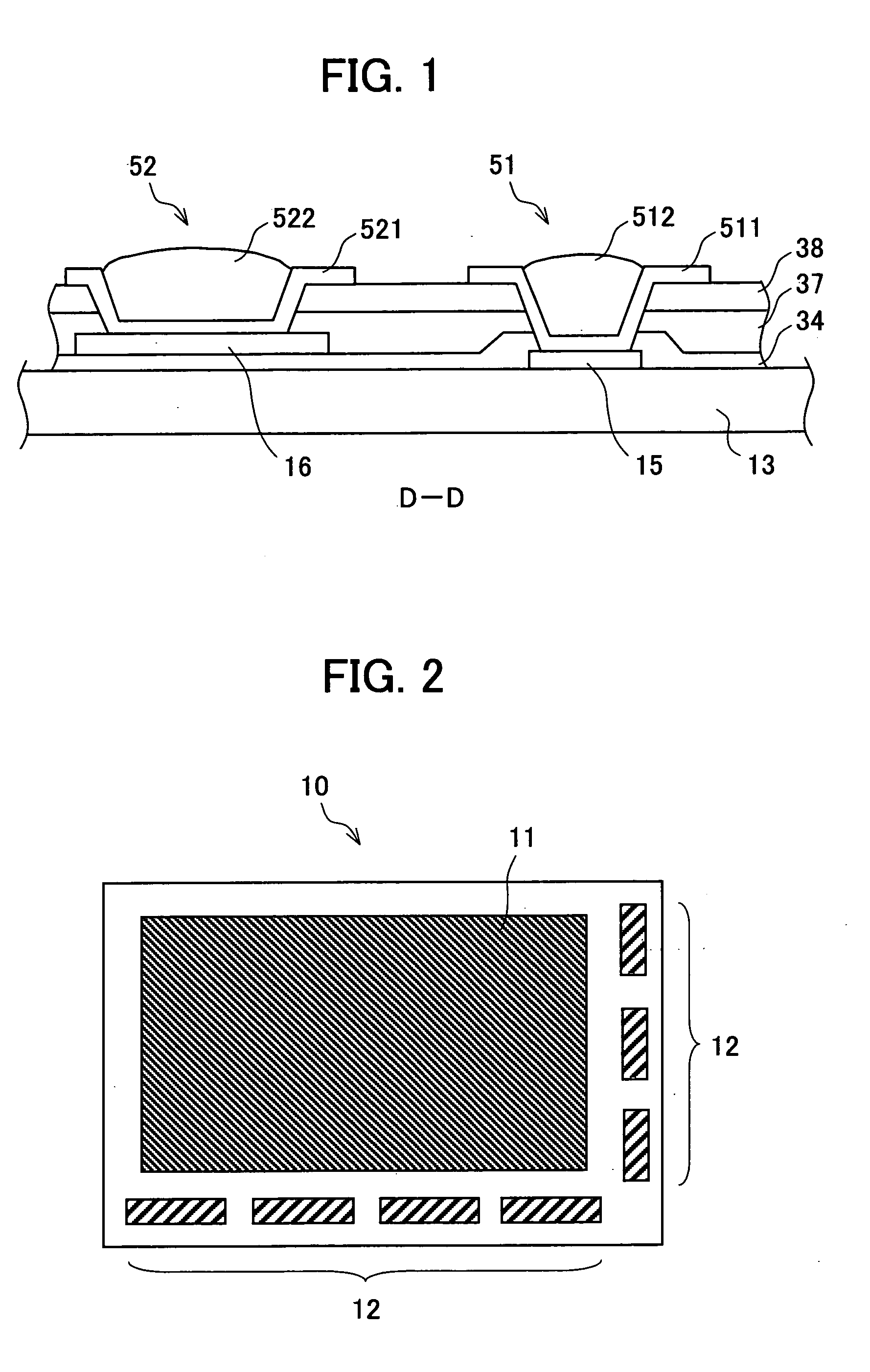
[0067]FIG. 2 is a plane view illustrating a schematic configuration of an active matrix substrate 10. As shown in FIG. 2, the active matrix substrate 10 includes an image forming region 11 and a panel-peripheral region 12. A plurality of gate lines and a plurality of source lines are arranged in the image forming region 11 so as to be orthogonal to each other. A pixel is provided in each region compartmentalized by a gate line and a source line, thereby allowing a plurality of pixels to be provided in a matrix-manner. The respective pixels provided in a matrix manner operate in the image forming region 11, thereby allowing the image forming region 11, in its entirety, to display images,

[0068] FIGS. 3 (a)...


PUM

PropertyMeasurementUnit
lengthaaaaaaaaaa
lengthaaaaaaaaaa
lengthaaaaaaaaaa

Abstract

An auxiliary line including a guide layer and an auxiliary metallic member is formed with respect to a signal transmitting line or a main auxiliary capacitance line formed on a glass substrate. The guide layer is formed in the same layer where pixel electrodes are formed. The auxiliary metallic member is formed by using a method such as an inkjet method, in which fine particles of metal is ejected or dropped.

Description

[0001] This Nonprovisional application claims priority under 35 U.S.C. § 119(a) on Patent Applications No. 2004 / 185191 filed in Japan on Jun. 23, 2004, and No. 2005 / 124254 filed in Japan on Apr. 21, 2005, the entire contents of which are hereby incorporated by reference. FIELD OF THE INVENTION [0002] The present invention relates to an active matrix substrate which has been widely used in a liquid crystal display, an organic electro luminescent display, or the like. BACKGROUND OF THE INVENTION [0003] An active matrix substrate has been used in, for example, a liquid crystal display and an organic EL (electro luminescent) display. This active matrix substrate conventionally includes metal wiring, such as signal lines and scanning lines, and pixel electrodes. The metal wiring and the pixel electrodes are generally formed as follows. Namely, a metal thin film is formed by carrying out a spattering method using a metal target, or an evaporation method. On this metal thin film, a mask is...

Claims


Application Information

Patent Timeline
Patent Type & Authority Applications(United States)
IPC IPC(8): G02F1/136G02F1/1362H01L27/32
CPCG02F1/136286G02F2001/13629H01L27/1292H01L27/3279H01L51/0022G02F2001/136295G02F1/13629G02F1/136295H10K59/1315H10K71/611G02F1/1345
Inventor AZUMADA, KYOKONAKAMURA, KENJIBAN, ATSUSHIFUJITA, TATSUYA
Owner SHARP KK
Why Eureka
Try Eureka