
Switch/network adapter port coupling a reconfigurable processing element to one or more microprocessors for use with interleaved memory controllers

a technology of interleaved memory controller and reconfigurable processing elements, which is applied in the direction of data conversion, instruments, digital computers, etc., can solve the problems of low potential sale volumes for any one chip set, high latency, and high cost of designing a new dedicated chip set that could provide such a port, so as to achieve the effect of double (or more) the width of the data bus into and out of memory

Inactive Publication Date: 2005-12-22
SRC COMP
View PDF34 Cites 22 Cited by
  • Summary
  • Abstract
  • Description
  • Claims
  • Application Information

AI Technical Summary

Benefits of technology

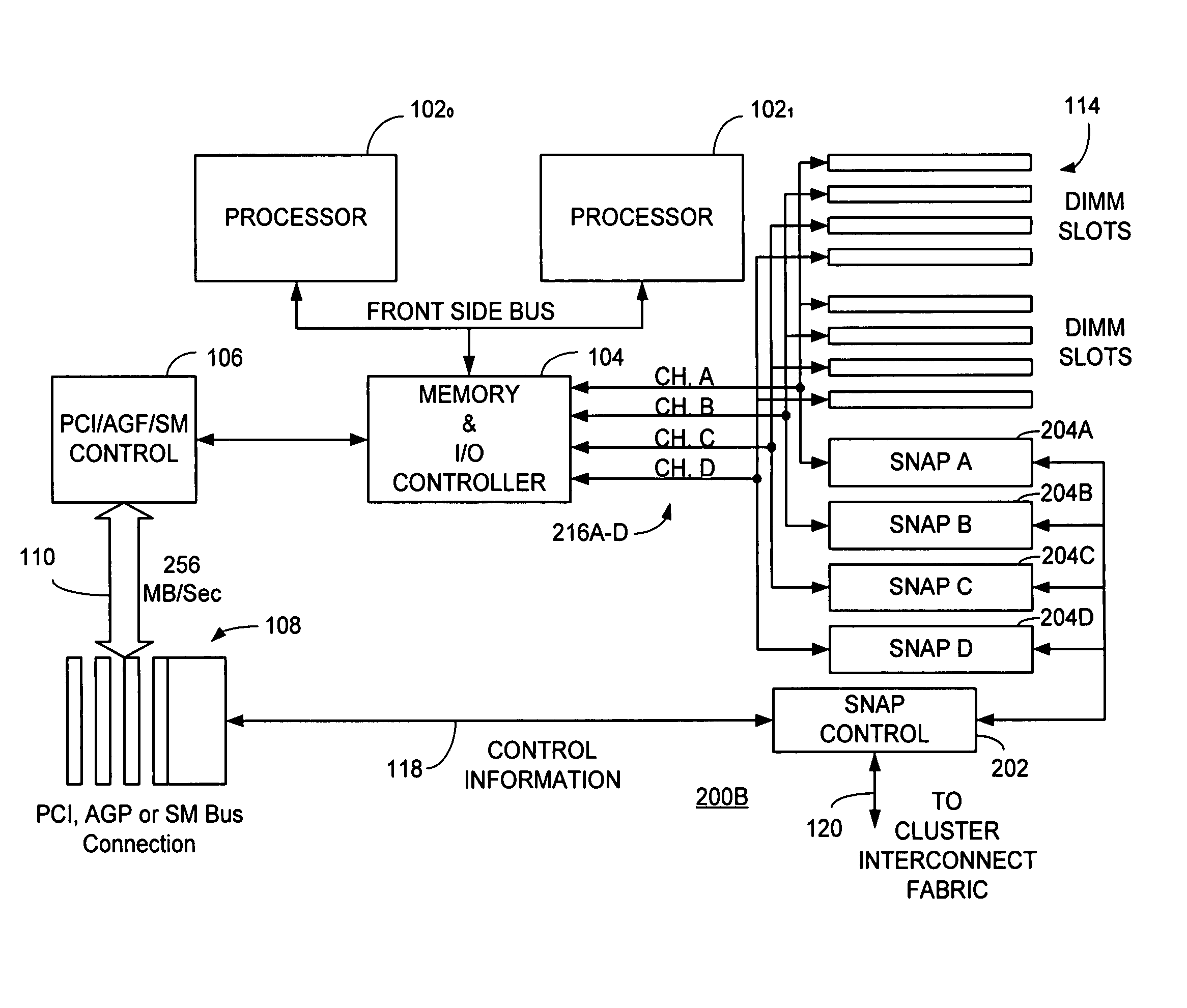
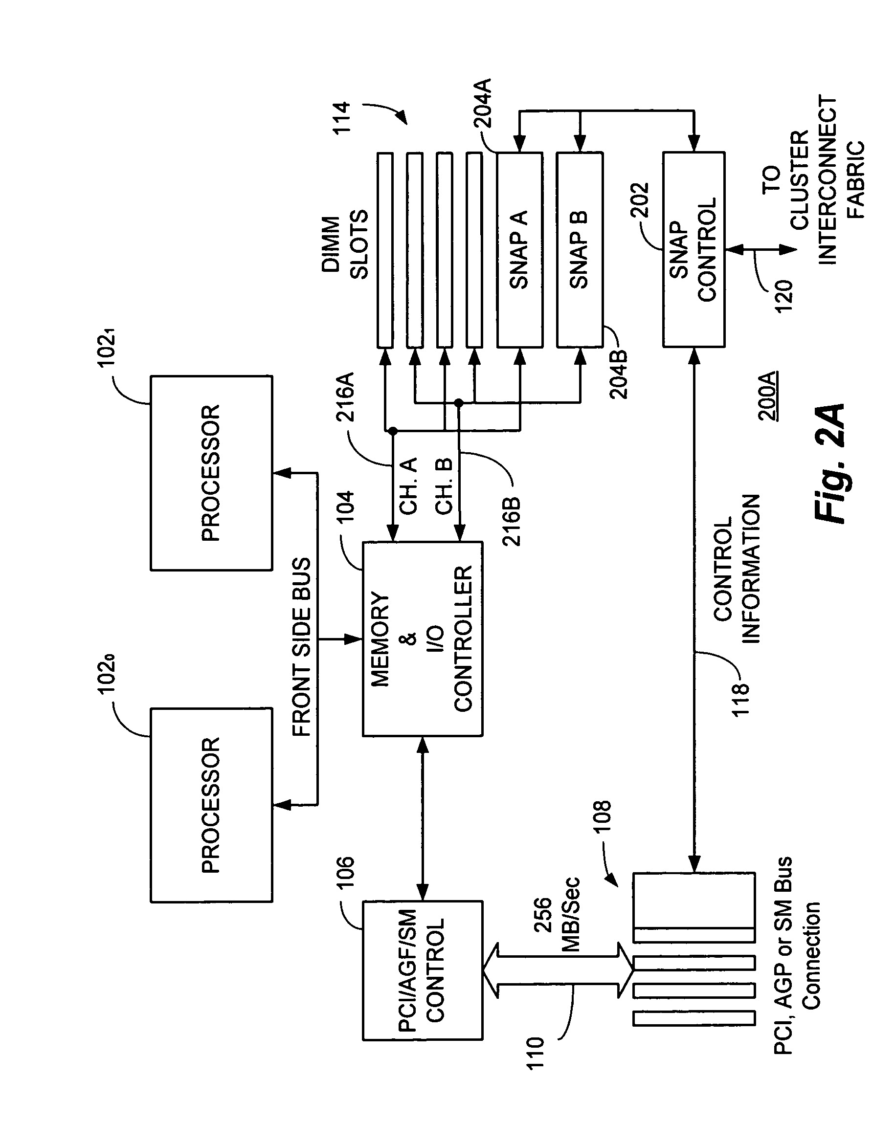
[0008] As disclosed in a representative embodiment herein, SRC Computers, Inc. proprietary SNAP™ technology has been enhanced such that the signals from two or more DIMM (or RIMM) slots are routed to a common control chip. Physically, in a by-two configuration, two DIMM form factor switch/network adapter boards may be coupled together using ridged flex circuit construction to form a single assembly. One of the DIMM boards may also be populated with a control field programmable gate array (“FPGA”) which may have the signals from both DIMM slots routed to it. The control chip then samples the data off of both slots using the independent clocks of the slots. The data from both slots is then used to form a data packet that is then sent to other parts of the system. In a similar manner, the technique disclosed herein may be utilized in conjunction with more than two DIMM slots, for example, four DIMM slots is an four-way interleaved system.
[0009] In accordance with the present invention, an interleaved memory system uses two or more memory channels running in lock-step. A connection is made to one of the DIMM slots and the signals derived are used ...

Problems solved by technology

While there are various versions of this bus available, all are limited to less than 1 GB / sec. bandwidth and, because of their location several levels of chips below the processor bus, they all exhibit a very high latency.
Unfortunately, designing a new, dedicated chip set that could provide such a port is not only very expensive, it would also have to be customized for each type of clustering interconnect encountered.
This would naturally lead to relatively low potential sale volumes for any one version of the chipset, thus rendering it cost ineffective.

Method used


Image

  • Switch/network adapter port coupling a reconfigurable processing element to one or more microprocessors for use with interleaved memory controllers
  • Switch/network adapter port coupling a reconfigurable processing element to one or more microprocessors for use with interleaved memory controllers
  • Switch/network adapter port coupling a reconfigurable processing element to one or more microprocessors for use with interleaved memory controllers

Examples


Embodiment Construction

[0025] With reference now to FIG. 1, a functional block diagram of an exemplary embodiment of a computer system 100 is shown comprising a switch / network adapter port for clustered computers employing a chain of multi-adaptive processors in a DIMM format to significantly enhance data transfer rates over that otherwise available from the peripheral component interconnect (“PCI”) bus.

[0026] In the particular embodiment illustrated, the computer system 100 includes one or more processors 1020 and 1021 which are coupled to an associated PC memory and I / O controller 104. In operation, the controller 104 sends and receives control information from a PCI control block 106. It should be noted that in alternative implementations of the present invention, the control block 106 may also be an accelerated graphics port (“AGP”) or system maintenance (“SM”) control block. The PCI control block 106 is coupled to one or more PCI card slots 108 by means of a relatively low bandwidth PCI bus 110 whic...


PUM


Abstract

A switch / network adapter port (“SNAP™”) in a dual in-line memory module (“DIMM”) or Rambus™ in-line memory module (“RIMM”) format for clustered computers employing multi-adaptive processor (“MAP®”, both trademarks of SRC Computers, Inc.) elements for use with interleaved memory controllers. Particularly disclosed is a microprocessor based computer system utilizing either a DIMM or RIMM physical format adapter port coupled to a reconfigurable processor element for the purpose of implementing a connection to an external switch, network, or other device. In a particular embodiment, connections may be provided to either the PCI, accelerated graphics port (“AGP”) or system maintenance (“SM”) bus for purposes of passing control information to the host microprocessor or other control chips. The field programmable gate array (“FPGA”) based processing elements have the capability to alter data passing through it to and from an external interconnect fabric or device.

Description

CROSS REFERENCE TO RELATED PATENT APPLICATIONS [0001] The present invention is a Continuation-In-Part of U.S. patent application Ser. No. 10 / 340,390 filed Jan. 10, 2003 for: “Switch / Network Adapter Port Coupling a Reconfigurable Processing Element to One or More Microprocessors for Use with Interleaved Memory Controllers”, U.S. patent application Ser. No. 09 / 932,330 filed Aug. 17, 2001 for: “Switch / Network Adapter Port for Clustered Computers Employing a Chain of Multi-Adaptive Processors in a Dual In-Line Memory Module Format” and U.S. Provisional Patent Application Ser. No 60 / 422,722 filed Oct. 31, 2002 for: “General Purpose Reconfigurable Computing Hardware and Software”, all of which are assigned to SRC Computers, Inc., Colorado Springs, Colo., the disclosures of which are herein specifically incorporated in their entirety by this reference.BACKGROUND OF THE INVENTION [0002] The present invention relates, in general, to the field of computer systems and methods incorporating one...

Claims


Application Information

Patent Timeline
IPC IPC(8): G06F13/00G06F13/16G06F13/38
CPCG06F13/385G06F13/1652
Inventor HUPPENTHAL, JON M.SEEMAN, THOMAS R.BURTON, LEE A.
Owner SRC COMP
Learn More