Apparatuses and methods for atomic layer deposition of hafnium-containing high-k dielectric materials

Inactive Publication Date: 2005-12-08
APPLIED MATERIALS INC
View PDF99 Cites 660 Cited by
  • Summary
  • Abstract
  • Description
  • Claims
  • Application Information

AI Technical Summary

Benefits of technology

[0013] In another embodiment, a method for forming a hafnium-containing dielectric stack on a substrate is provided which includes forming at least one hafnium oxide layer and at least one hafnium silicate layer. The method includes sequentially exposing the substrate to the oxidizing gas and a first process gas containing a hafnium precursor to form a first hafnium-containing material thereon and sequentially exposing the substrate to the oxidizing gas and a second process gas containing the hafnium precursor to form a second hafnium-containing material on the first hafnium-containing material. In one example, the first process gas also contains a silicon precursor. The method further includes forming an oxidizing gas containing water vapor by flowing a hydrogen source gas and an oxygen source gas into a water vapor generator.

Problems solved by technology

While conventional chemical vapor deposition (CVD) has proved successful for device geometries and aspect ratios down to 0.15 μm, the more aggressive device geometries require an alternative deposition technique.
While the high reactivity at low temperature is an attribute of the radical oxidizing agents, undesirable side reactions are prevalent throughout the process chamber forming contaminants on the substrate.
However, due to the moderate reactivity of water or oxygen, ALD processes generally require slower flow rates, longer exposure periods and higher temperatures than radical oxygen sources.
Furthermore, the slow flow rates and high temperatures usually increase contaminants on the substrate surface.
While the aforementioned steam oxidation processes may produce an effective water vapor for use during a CVD process, the generated water vapor is not acceptable for use during an ALD process.
Water vapor derived from these steam oxidation processes may cause contaminants on the substrate surface and modest control over process temperature or the contents of the oxidizing water vapor.

Method used


Image

  • Apparatuses and methods for atomic layer deposition of hafnium-containing high-k dielectric materials
  • Apparatuses and methods for atomic layer deposition of hafnium-containing high-k dielectric materials
  • Apparatuses and methods for atomic layer deposition of hafnium-containing high-k dielectric materials

Examples


example 1

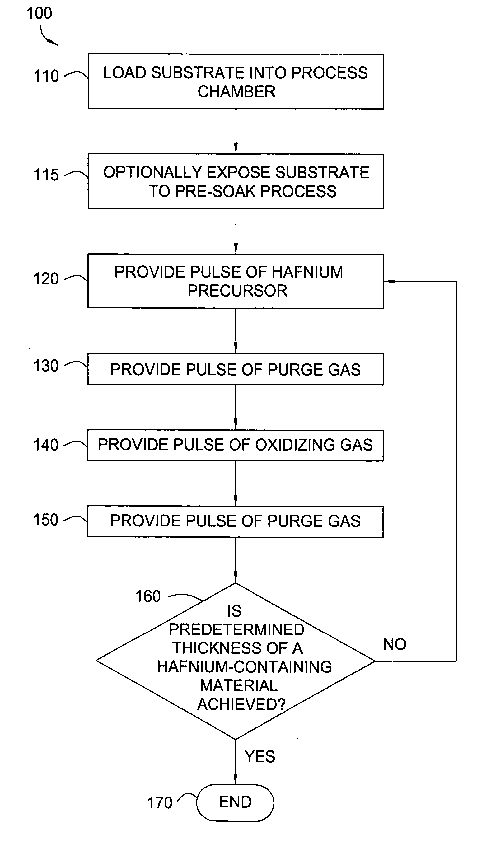
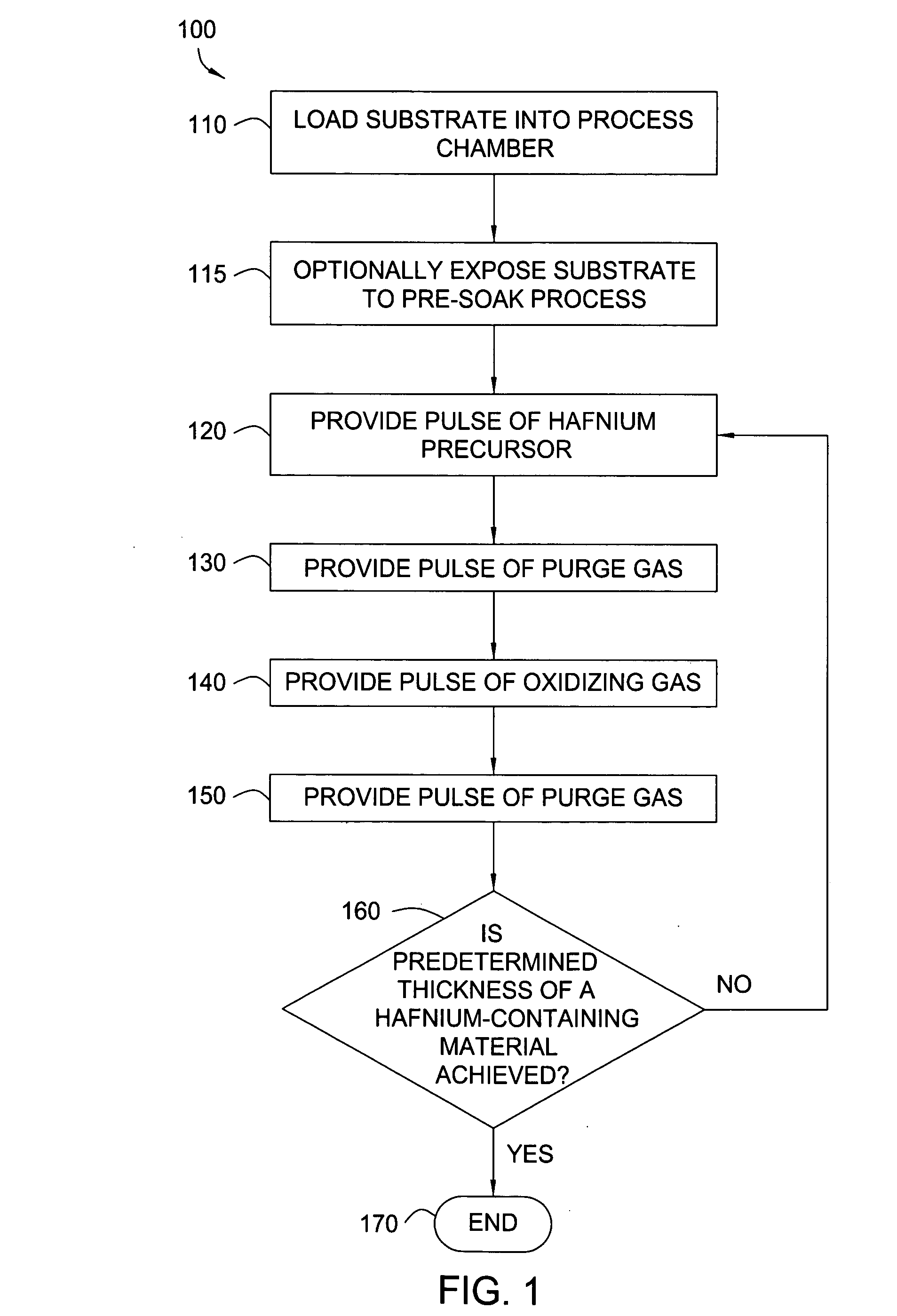
[0129] A hafnium oxide film is formed during an ALD process by sequentially pulsing a hafnium precursor with an oxidizing gas produced by a WVG system. A substrate surface is exposed to a pretreatment process to form hydroxyl groups thereon. The hafnium precursor, HfCl4, is heated within a precursor ampoule at a temperature in a range from about 150° C. to about 200° C. A nitrogen carrier gas is directed into the precursor ampoule containing the hafnium precursor with a flow rate of about 400 sccm. The hafnium precursor saturates the carrier gas and is provided into the chamber for about 3 seconds. A purge gas of nitrogen is provided into the chamber for about 2.5 seconds to remove any unbound hafnium precursor. Hydrogen gas and oxygen gas with the flow rate of about 100 sccm and about 120 sccm respectively, are supplied to the WVG system. The oxidizing gas coming from the WVG system contains water with a flow rate of about 100 sccm and oxygen with a flow rate of about 70 sccm. The ...

example 2

[0130] A hafnium oxide film is formed during an ALD process by sequentially pulsing a hafnium precursor with an oxidizing gas. A substrate surface is exposed to a pretreatment process to form hydroxyl groups thereon. The hafnium precursor, HfCl4, is heated within a precursor ampoule at a temperature in a range from about 150° C. to about 200° C. A nitrogen carrier gas is directed into the precursor ampoule containing the hafnium precursor with a flow rate of about 400 sccm. The hafnium precursor saturates the carrier gas and is provided into the chamber for about 0.5 seconds. A purge gas of nitrogen is provided into the chamber for about 0.5 seconds to remove any unbound hafnium precursor. Hydrogen gas and oxygen gas with the flow rate of about 50 sccm and about 60 sccm respectively, are supplied to the WVG system. The oxidizing gas coming from the WVG system contains water with a flow rate of about 50 sccm and oxygen with a flow rate of about 35 sccm. The oxidizing gas is provided ...

example 3

[0131] A hafnium silicate film is formed during with an ALD process by sequentially pulsing a hafnium precursor with an oxidizing gas followed by pulsing a silicon precursor with the oxidizing gas. A substrate surface is exposed to a pretreatment process to form hydroxyl groups thereon. The hafnium precursor, TDEAH, and silicon precursor, TDMAS, are heated within separate precursor ampoules at room temperature (about 23° C.). These precursors are vaporized individually in vaporizers at about 110° C. to about 130° C. and individually mixed with an inert carrier gas. The hafnium precursor saturates the carrier gas and is provided into the chamber for about 1 second. A purge gas of nitrogen is provided into the chamber for about 1 second to remove any unbound hafnium precursor. Hydrogen gas and oxygen gas with the flow rate of about 100 sccm and about 120 sccm respectively, are supplied to the WVG system. The oxidizing gas coming from the WVG system contains water with a flow rate of a...


PUM

PropertyMeasurementUnit
Timeaaaaaaaaaa
Timeaaaaaaaaaa
Dielectric polarization enthalpyaaaaaaaaaa

Abstract

Embodiments of the invention provide methods for depositing dielectric materials on substrates during vapor deposition processes, such as atomic layer deposition (ALD). In one example, a method includes sequentially exposing a substrate to a hafnium precursor and an oxidizing gas to deposit a hafnium oxide material thereon. In another example, a hafnium silicate material is deposited by sequentially exposing a substrate to the oxidizing gas and a process gas containing a hafnium precursor and a silicon precursor. The oxidizing gas usually contains water vapor formed by flowing a hydrogen source gas and an oxygen source gas through a water vapor generator. In another example, a method includes sequentially exposing a substrate to the oxidizing gas and at least one precursor to deposit hafnium oxide, zirconium oxide, lanthanum oxide, tantalum oxide, titanium oxide, aluminum oxide, silicon oxide, aluminates thereof, silicates thereof, derivatives thereof or combinations thereof.

Description

CROSS-REFERENCE TO RELATED APPLICATIONS [0001] This application claims benefit of U.S. Provisional Patent Application Ser. No. 60 / 570,173, entitled, “Atomic Layer Deposition of Hafnium-containing High-k Materials,” filed May 12, 2004, which is herein incorporated by reference in its entirety.BACKGROUND OF THE INVENTION [0002] 1. Field of the Invention [0003] Embodiments of the invention generally relate to methods and apparatuses for depositing materials on a substrate, and more specifically, to methods and apparatuses for depositing high-k dielectric materials by vapor deposition processes. [0004] 2. Description of the Related Art [0005] In the field of semiconductor processing, flat-panel display processing or other electronic device processing, vapor deposition processes have played an important role in depositing materials on substrates. As the geometries of electronic devices continue to shrink and the density of devices continues to increase, the size and aspect ratio of the f...

Claims


Application Information

Patent Timeline
IPC IPC(8): C23C16/00C23C16/02C23C16/40C23C16/44C23C16/448C23C16/455C23C16/56F22B1/00
CPCC23C16/0272C23C16/40C23C16/401C23C16/405C23C16/4412C23C16/4488C23C16/45529C23C16/45531C23C16/45544C23C16/45582C23C16/56Y02T50/67Y10T137/0396Y10T137/2087Y10T137/0357C23C16/00Y02T50/60
Inventor KHER, SHREYASNARWANKAR, PRAVINSHARANGAPANI, RAHUL
Owner APPLIED MATERIALS INC
Why Eureka
Try Eureka