Eureka AIR delivers breakthrough ideas for toughest innovation challenges, trusted by R&D personnel around the world.

Semiconductor device and manufacturing method therefor

a semiconductor device and manufacturing method technology, applied in the direction of semiconductor devices, semiconductor/solid-state device details, electrical devices, etc., can solve the problem of becoming difficult to ensure the wire bond region, and achieve the effect of enhancing the heat radiation efficiency of semiconductor devices

Active Publication Date: 2005-11-24
MURATA MFG CO LTD
View PDF8 Cites 23 Cited by
  • Summary
  • Abstract
  • Description
  • Claims
  • Application Information

AI Technical Summary

Benefits of technology

[0017] An object of the present invention is to provide a semiconductor device whose size can be reduced.
[0018] Another object of the present invention is to provide a semiconductor device with enhanced heat radiation efficiency.
[0024] Semiconductor devices can be reduced in size. The heat radiation efficiency of semiconductor devices can be enhanced.

Problems solved by technology

As downsizing of power amplifier modules progresses, as mentioned above, it is becoming difficult to ensure wire bond regions where a semiconductor chip and a wiring substrate are electrically connected with each other.

Method used


Image

  • Semiconductor device and manufacturing method therefor
  • Semiconductor device and manufacturing method therefor
  • Semiconductor device and manufacturing method therefor

Examples


Embodiment Construction

[0043] In the following description of the embodiment, it will be divided into a plurality of sections or embodiments if necessary for the sake of convenience. However, they are not regardless of each another, but are in such a relation that one is a modification to, the details of, the supplementary explanation of, or the like of part or all of the other unless otherwise stated.

[0044] If reference is made to any number of elements or the like (including number of pieces, numeric value, quantity, range, and the like) in the description of the embodiment below, the present invention is not limited by that value. The number may be greater or less than the value. However, the following cases are excepted: cases where some number is explicitly specified, cases where some number is evidently limited to a specific value in principle, and the like cases.

[0045] In the embodiment described below, needless to add, their components (including constituent steps and the like) are not necessari...


PUM


Abstract

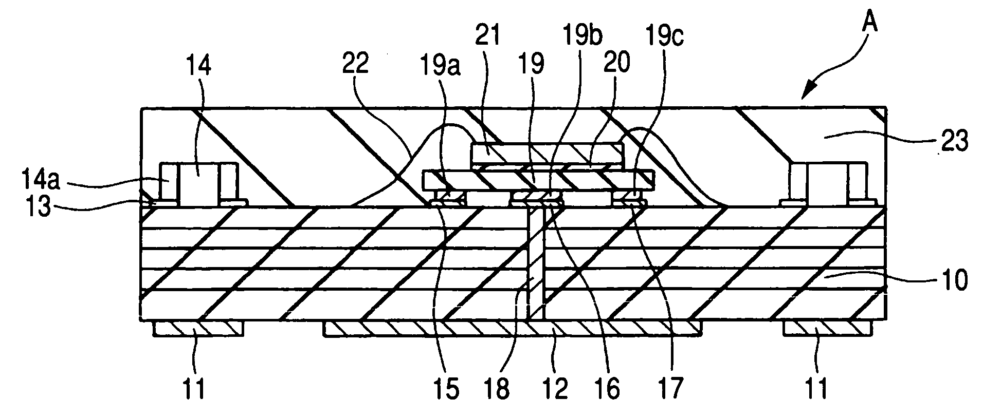
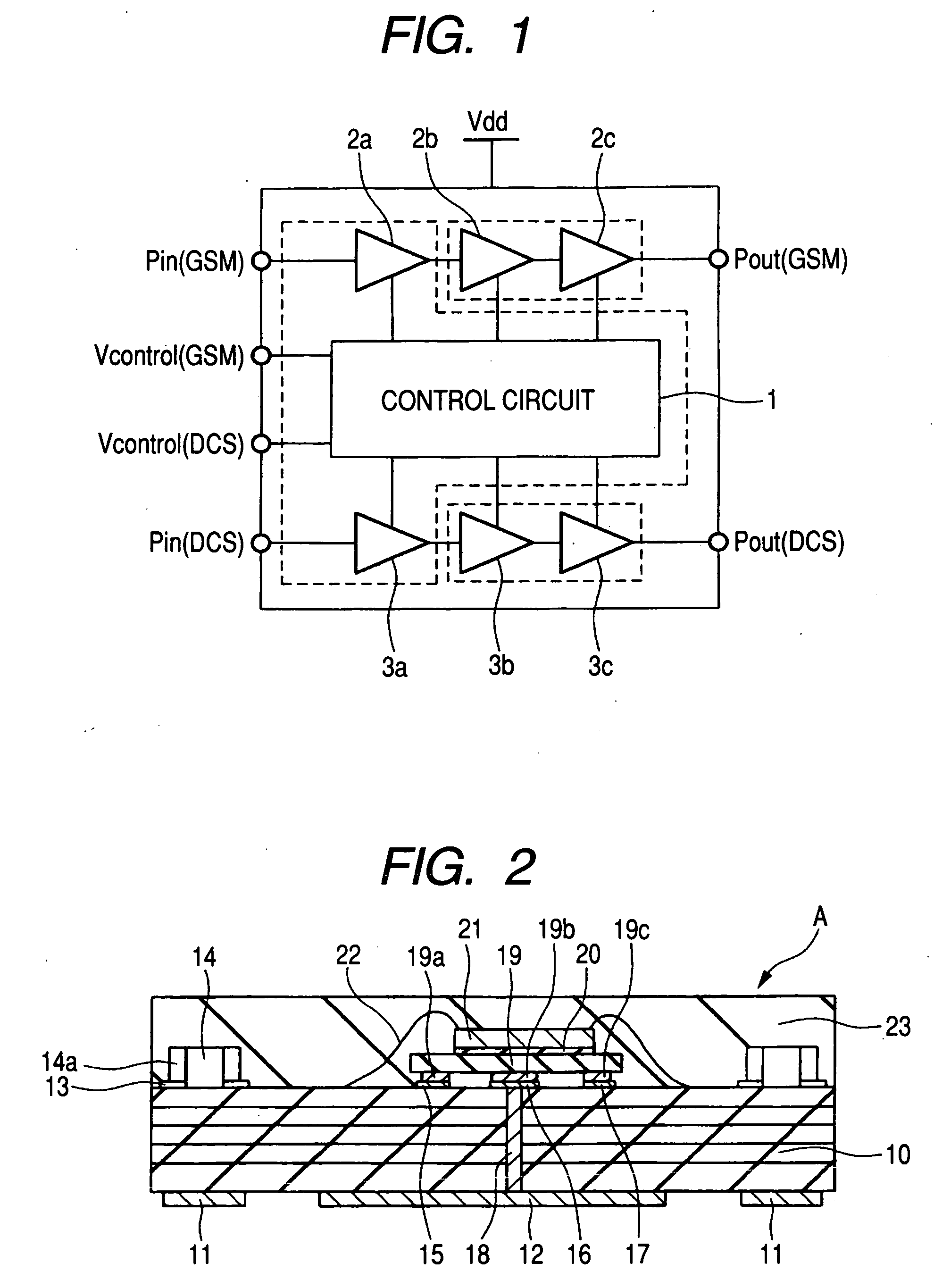
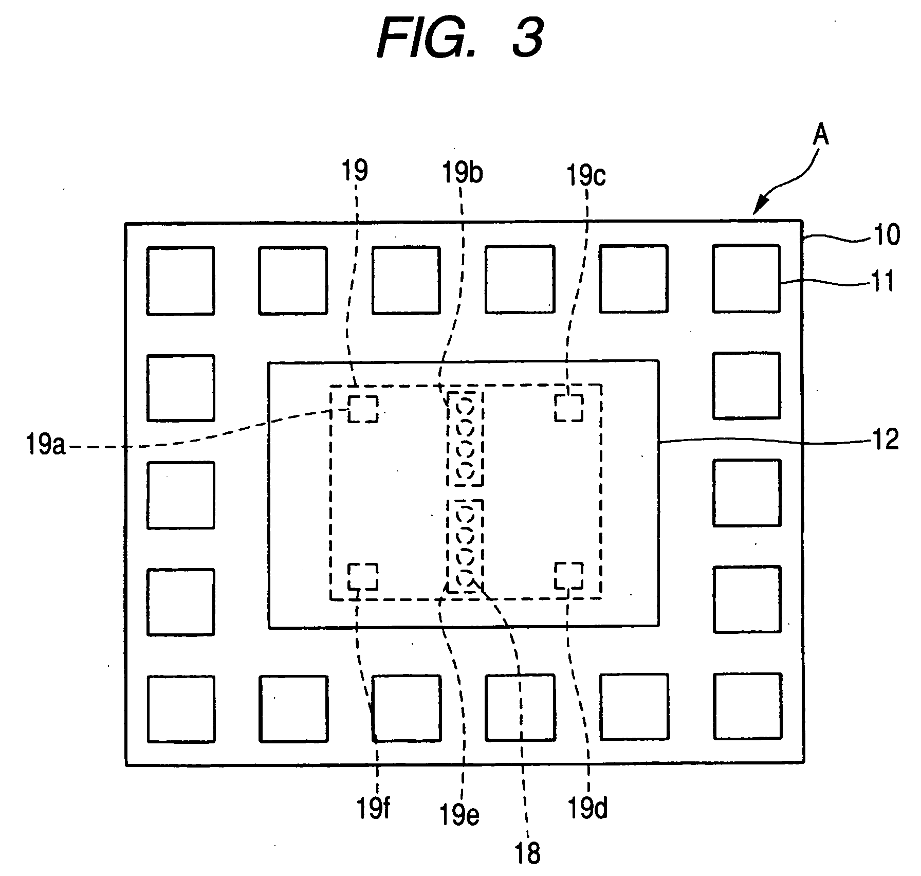
A semiconductor device has an external wiring for GND formed over an underside surface of a wiring substrate. A plurality of via holes connecting to the external wiring for GND are formed to penetrate the wiring substrate. A first semiconductor chip of high power consumption, including HBTs, is mounted over a principal surface of the wiring substrate. The emitter bump electrode of the first semiconductor chip is connected in common with emitter electrodes of a plurality of HBTs formed in the first semiconductor chip. The emitter bump electrode is extended in a direction in which the HBTs line up. The first semiconductor chip is mounted over the wiring substrate so that a plurality of the via holes are connected with the emitter bump electrode. A second semiconductor chip lower in heat dissipation value than the first semiconductor chip is mounted over the first semiconductor chip.

Description

CROSS-REFERENCE TO RELATED APPLICATION [0001] The present application claims priority from Japanese patent application No. 2004-142506 filed on May 12, 2004, the content of which is hereby incorporated by reference into this application. BACKGROUND OF THE INVENTION [0002] The present invention relates to a semiconductor device and a manufacturing technique for the semiconductor device, and more particularly to a technology effectively applicable to a semiconductor device including HBTs (Heterojunction Bipolar Transistors) and a manufacturing technique for the semiconductor device. [0003] For example, there are semiconductor elements using III-V compound semiconductor such as gallium arsenide (GaAs). The compound semiconductor is characterized in that it is higher in mobility than silicon (Si) and half-insulating crystals are obtained. In the compound semiconductor, mixed crystals can created, and heterojunctions can be formed. [0004] One of semiconductor elements using heterojunctio...

Claims


Application Information

Patent Timeline
Patent Type & Authority Applications(United States)
IPC IPC(8): H01L21/331H01L21/28H01L21/8222H01L21/84H01L23/34H01L23/482H01L23/498H01L25/065H01L25/07H01L25/16H01L25/18H01L27/082H01L29/417H01L29/423H01L29/45H01L29/49H01L29/737H01L29/739H01L29/78
CPCH01L21/84H01L23/4824H01L2924/1305H01L2224/16235H01L2224/1703H01L2224/1403H01L2924/13091H01L24/49H01L24/48H01L2924/3011H01L2924/30107H01L2924/19105H01L2924/19041H01L2924/1517H01L2924/15153H01L23/49844H01L25/16H01L29/456H01L29/4933H01L29/7835H01L2224/32145H01L2224/48091H01L2224/48227H01L2224/49171H01L2224/49175H01L2224/73253H01L2224/73265H01L2924/01078H01L2924/01079H01L2924/00014H01L2924/00H01L2924/00012H01L2924/30111H01L24/73H01L2924/181H01L2224/45099H01L2224/45015H01L2924/207
Inventor KONISHI, SATORUENDO, TSUNEONAKAJIMA, HIROKAZUUMEMOTO, YASUNARISASAKI, SATOSHIKUSANO, CHUSHIROIMAMURA, YOSHINORIKUROKAWA, ATSUSHI
Owner MURATA MFG CO LTD
Why Eureka
Eureka Blog
Learn More