
MRAM element

a random access and memory element technology, applied in information storage, static storage, digital storage, etc., can solve the problems of increasing memory density, increasing difficulty, and reducing process reliability, and achieve the effect of high density of memory cells

Active Publication Date: 2005-10-27
STMICROELECTRONICS SRL +2
View PDF9 Cites 13 Cited by
  • Summary
  • Abstract
  • Description
  • Claims
  • Application Information

AI Technical Summary

Benefits of technology

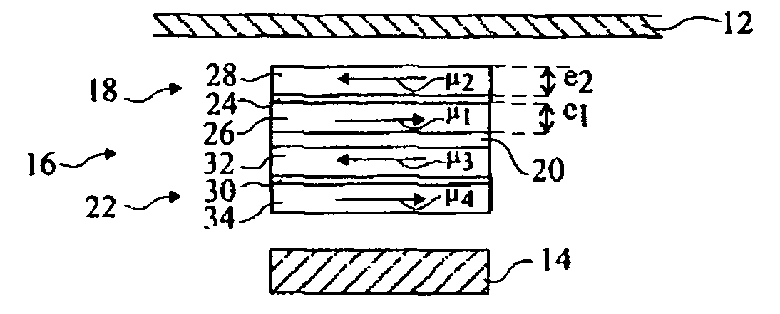
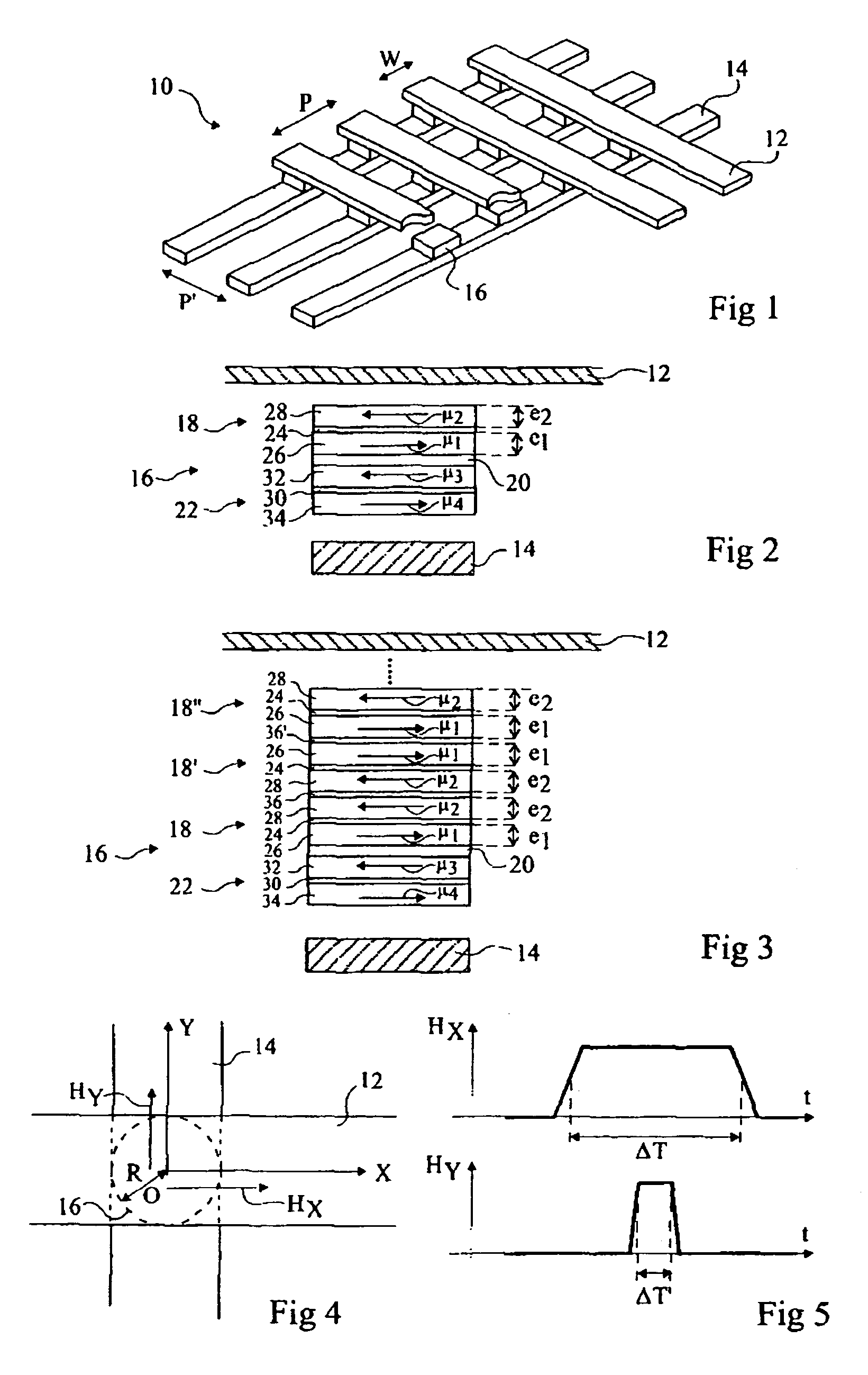
[0021] The present invention aims at obtaining a specific compensated or almost compensated memory element structure, especially intended for use in a MRAM, enabling direct writing, with no previous reading, of information into the memory element by means of currents having moderate amplitudes, and enabling pushing back the previously-described limits for obtaining a high density of memory cells.

Problems solved by technology

A difficulty results due to the fact that, by dipolar interaction, the magnetic moment of a considered memory element is likely to disturb the behavior of adjacent memory elements, the difficulty increases as the memory density increases.
A disturbance for example translates as a degradation in the reliability of the process of information writing into the memory elements adjacent to the considered memory element, or as a degradation in the information retention time in the adjacent memory elements.
The obtaining of proper write magnetic fields is generally more difficult still when the free magnetic region of the memory element has a compensated or almost compensated structure since the modification of the orientation of the magnetic moment vectors of the memory elements tends to require more intense magnetic fields, in particular to overcome the interaction between the layers of the free magnetic region.
Further, when a magnetic field is applied to the memory element, it is difficult to ensure that resulting moment {right arrow over (μ)}tot of free magnetic region 18 maintains during the write process a sufficiently low amplitude to avoid disturbing the adjacent memory elements.

Method used


Image

  • MRAM element
  • MRAM element
  • MRAM element

Examples


Embodiment Construction

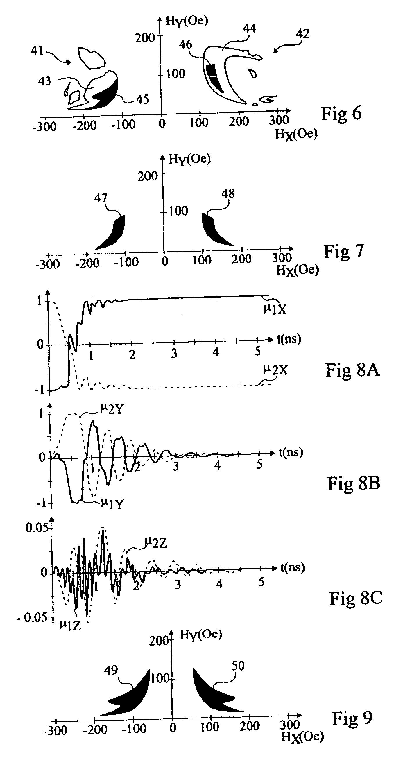
[0042] The applicant has determined, by many trials and simulations, that by providing a dissymmetry of certain magnetic properties of the ferromagnetic layers forming the free magnetic region of the memory element, it is possible to perform a direct writing into the memory element, even with a compensated structure, by using write magnetic fields of moderate amplitudes.

[0043] According to a first example of implementation of the write method according to the present invention, which will be described in further detail hereafter, it is desired to obtain a compensated or almost compensated magnetic region for which one of the following properties or the following two properties are different: [0044] the anisotropy fields of crystallographic origin; [0045] the demagnetizing field tensors.

[0046]“Demagnetizing field tensor” is used to designate the tensor having its matrix product with the direction cosines of the magnetization of the ferromagnetic layer providing the demagnetizing fi...


PUM


Abstract

A magnetoresistive memory element including a trapped magnetic region and a free magnetic region separated by a barrier layer. The free magnetic region comprises a stacking of at least two antiferromagnetically-coupled ferromagnetic layers, a layer magnetic moment vector being associated with each layer, the resulting magnetic moment vector, equal to the sum of the layer magnetic moment vectors, having an amplitude smaller than at least 40% of the amplitude of the layer magnetic moment vector of maximum amplitude. The anisotropy field and / or the demagnetizing field tensor is not identical for the at least two ferromagnetic layers, whereby the angular deviations of the layer magnetic moment vectors are different at the time of the application of an external magnetic field, which enables at least two methods for directly writing into the memory element, as well as its initialization.

Description

BACKGROUND OF THE INVENTION [0001] 1. Field of the Invention [0002] The present invention relates to a Magnetic Random Access Memory (MRAM) element, and especially to a memory element to be used in a MRAM comprising an array of memory elements. [0003] 2. Description of the Related Art [0004] A MRAM element is generally characterized by a magnetic moment vector having an orientation that can be modified by the application of an external action, especially a magnetic field. Specific information is stored in the memory element by orienting the magnetic moment vector along a selected direction and / or orientation. The memory element can keep information for a long time without requiring refreshment of the memory element in the absence of a power supply, which is a significant advantage of this type of memory. As an example, to store binary information, a memory element having a selected-magnetization axis may be provided. The magnetic moment vector is then oriented along a selected-magne...

Claims


Application Information

Patent Timeline
IPC IPC(8): G11C11/16
CPCG11C11/16
Inventor KIM, JOO-VONDEVOLDER, THIBAUTCHAPPERT, CLAUDEMAUFRONT, CEDRICFOURNEL, RICHARD
Owner STMICROELECTRONICS SRL
Learn More