
Led lighting assembly

a technology for led lamps and assembly parts, applied in the field of new, can solve the problems of high power consumption requirements, manufacturing difficulties, and damage to the emitter chip and the circuitry required to drive the led, and achieve the effect of reducing the cost of manufacturing and assembly

Inactive Publication Date: 2005-09-15
OPTICAL RES ASSOCS
View PDF40 Cites 92 Cited by
  • Summary
  • Abstract
  • Description
  • Claims
  • Application Information

AI Technical Summary

Benefits of technology

[0010] The outer enclosure of the present invention is preferably formed from the same material as the inner mounting die. In the preferred embodiment, this is brass but may be thermally conductive polymer or other metallic materials. The outer enclosure slides over the inner mounting die and has a circular opening in the top end that receives the clear optical portion of the Luxeon LED package therethrough. The outer enclosure serves to further transfer heat from the inner mounting die and the LED package, as it is also highly thermally conductive and in thermal communication with both the inner mounting die and the LED package. The outer enclosure also covers the groove in the side of the inner mounting die protecting the insulator strip and circuitry mounted thereon from damage.
[0012] Finally, the present invention in another embodiment provides for an optical assembly that is well suited for use in conjunction with an LED package wherein a high percentage of the light output from the LED is collected and directed forward in a manner that allows the light to be coupled into a light conduit.
[0013] Accordingly, one of the objects of the present invention is the provision of an optical assembly for coupling a high intensity LED with a light conduit. Another object of the present invention is the provision of an assembly for coupling a high intensity LED with a light conduit that is highly efficient and serves to transfer a high percentage of the LED light output into the light conduit. Yet a further object of the present invention is the provision of an assembly for packaging a high intensity LED that includes integral means for coupling the LED with a light conduit using a one piece optical assembly that captures both the on axis and lateral luminous output and collimates the output to create a homogenous beam image at the input end of the light conduit. A further object of the present invention is the provision of an assembly for packaging a high intensity LED that includes an integrated optical assembly that creates a homogenous and focused beam image at the output face thereof that is further coupled into a light conduit.

Problems solved by technology

These high brightness packages differ from conventional LED lamps in that they use emitter chips of much greater size, which accordingly have much higher power consumption requirements.
However, due to their unique shape, size and power consumption requirements they present manufacturing difficulties that were originally unanticipated by the LED manufacturers.
If this heat is not effectively dissipated, it may cause damage to the emitter chip and the circuitry required to drive the LED.
While these assemblies are effective in properly cooling the LED package, they are generally bulky and difficult to incorporate into miniature flashlight devices.
Further, since the circuit boards that have these heat transfer plates include a great deal of heat sink material, making effective solder connections to the boards is difficult without applying a large amount of heat.
Ultimately however, these assemblies malfunction due to overheating of the emitter chip, since the heat generated cannot be dissipated.
Further, because of the large form factor of the emitter chip in these assemblies they tend to emit light over a wide output angle.
While this is the common approach used in the manufacture of compact lighting devices such as flashlights, this method includes several inherent drawbacks.
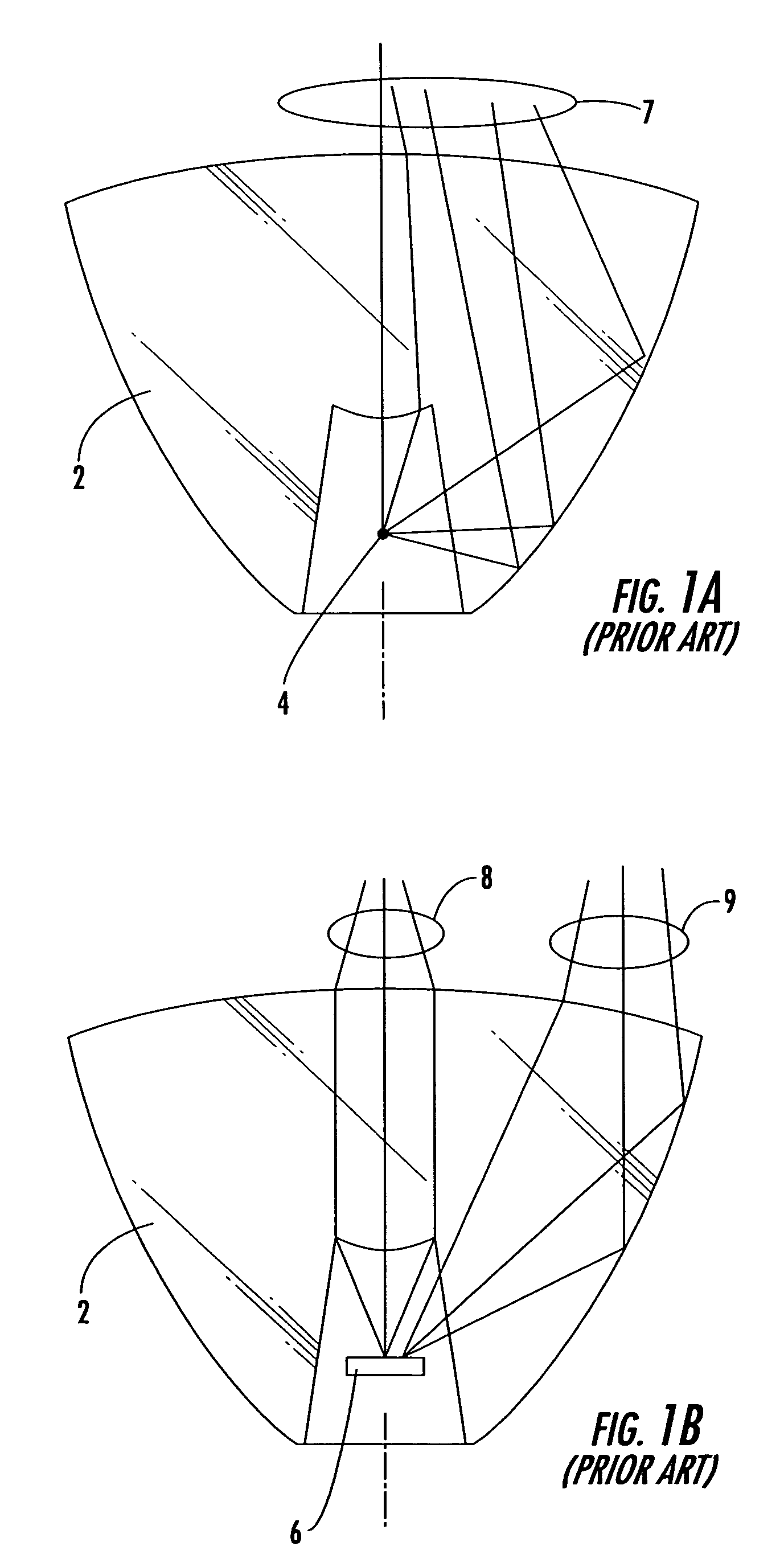
First, while this arrangement can capture much of the output radiation from the light source, the captured output is only slightly collimated.
The drawback is that when a lens of this type is used, the image of the light source is directly transferred into the far field of the beam.
Second, the light output is not well homogenized using an arrangement of this type.
Often this direct transfer of the light source image creates a rough appearance to the beam that is unattractive and distracting for the user of the light.
Third, most of these configurations are inefficient and transfer only a small portion of the radiational output into the on axis output beam of the lighting device.
In this manner, these devices create additional manufacturing and assembly steps that increase the overall cost of the device and increase the chance of defects.
A clear limitation is that when it is used with a real extended source 6 of appreciable surface area (such as an LED chip) as seen in FIG. 1B, the collimation is incomplete and the output is directed into a diverging conic beam that includes a clear image of the chip as a central high intensity region 8 and a secondary halo region 9.

Method used


Image

  • Led lighting assembly
  • Led lighting assembly
  • Led lighting assembly

Examples


Embodiment Construction

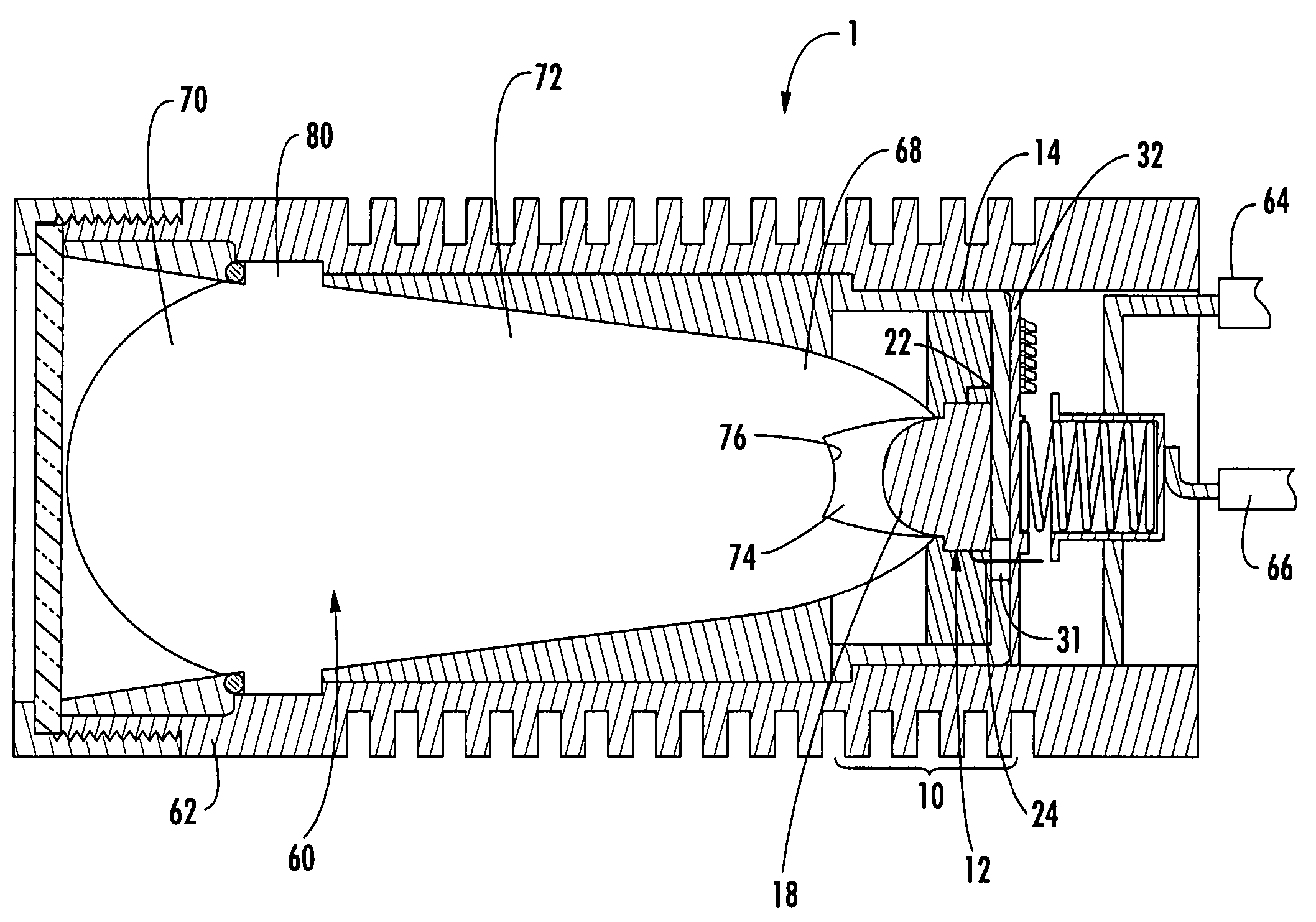
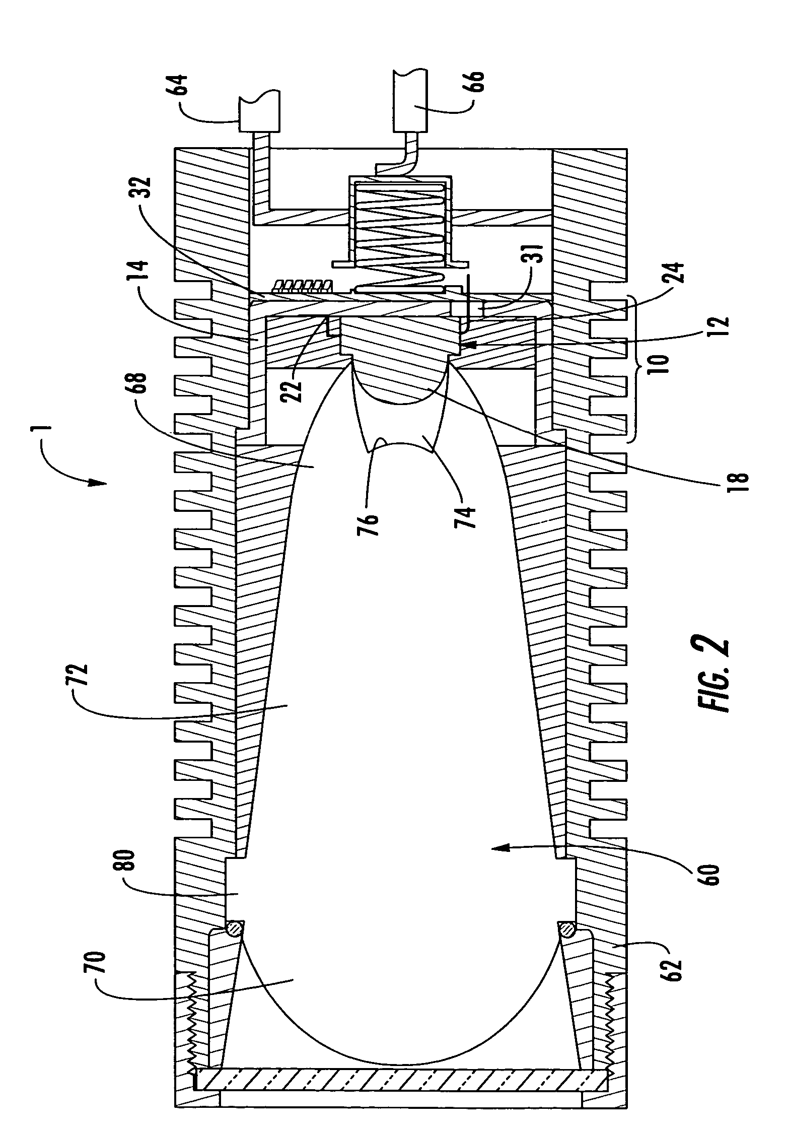
[0046] Referring now to the drawings, the light emitting diode (LED) lighting assembly of the present invention is illustrated and generally indicated at 1. The lighting assembly 1 generally includes an LED and heat sink sub-assembly 10 and an optical assembly 60 that are contained and maintained in spaced relation within an outer housing 62. As will hereinafter be more fully described, the present invention illustrates an LED lighting assembly 1 for further incorporation into a lighting device. For the purposes of providing a preferred embodiment of the present invention, the device 1 will be shown incorporated into a generic housing 62 with two power supply leads 64, 66 extending therefrom, however, the present invention also may be incorporated into any other lighting device such as architectural specialty lighting, vehicle lighting, portable lighting or flashlights. In general, the present invention provides a means for packaging a high intensity LED lamp that includes integral ...


PUM


Abstract

The present invention provides an optical lens for coupling the light output from a high intensity light source, such as an LED, with a light conduit. The optical lens captures, homogenizes and transmits substantially all of the light emitted the light source to a point of convergence that is centrally located on the output face of the optical lens. The present invention transmits upwards of 85% of the light emitted by the light source and produces a uniformly illuminated circular focal point that is easily discharged into the terminal end of an optical conduit such as an optical fiber of light pipe. Optionally the lens may be formed to include structure that serves to receive and retain the terminal end of the optical conduit.

Description

CROSS-REFERENCE TO RELATED APPLICATIONS [0001] This application is related to and is a continuation-in-part of U.S. patent application Ser. No. 10 / 731,392, filed Dec. 9, 2003, which is a continuation-in-part of U.S. patent application Ser. No. 10 / 658,613, filed Sep. 8, 2003, now U.S. Pat. No. 6,819,505.BACKGROUND OF THE INVENTION [0002] The present invention relates to a new assembly for coupling a high intensity LED lamp with a light conduit. More specifically, this invention relates to an assembly for coupling a high intensity LED lamp to a light conduit using an high efficiency optical control element. [0003] Currently, several manufacturers are producing high brightness light emitting diode (LED) packages in a variety of forms. These high brightness packages differ from conventional LED lamps in that they use emitter chips of much greater size, which accordingly have much higher power consumption requirements. In general, these packages were originally produced for use as direct...

Claims


Application Information

Patent Timeline
Patent Type & Authority Applications(United States)
IPC IPC(8): H01L27/00
CPCH01L33/58G02B6/4206G02B6/4214F21V5/04F21V29/713F21Y2101/02G02B7/026G02B19/0028G02B19/0061F21V7/0091F21Y2115/10
Inventor CASSARLY, WILLIAM JAMESGALLI, ROBERT D.
Owner OPTICAL RES ASSOCS
Learn More