
Method and apparatus for determining characteristics of thin films and coatings on substrates

a technology applied in the direction of mechanical measurement arrangements, mechanical roughness/irregularity measurements, instruments, etc., can solve the problems of inability to accurately measure the properties of thin films and coatings, high contact pressure, and significant stress deep in the substra

Inactive Publication Date: 2005-08-11
NEVMET CORP
View PDF4 Cites 30 Cited by
  • Summary
  • Abstract
  • Description
  • Claims
  • Application Information

AI Technical Summary

Benefits of technology

[0012] The object of the present invention is to provide a durability test method and test apparatus for reliable testing and measurement of characteristics in thin and ultra-thin films and coatings on substrates and under-layers. Another object is to provide the aforementioned method and apparatus that allow for reliable interpretation of test and measurement data. Still another object is to provide the aforementioned method and apparatus for measuring characteristics of films and coatings having a thickness of the order of nanometers to tens of nanometers. A further object is to provide the aforementioned method and apparatus that are based on electrical measurements. Still another object is to provide an apparatus suitable for measuring characteristics of both conductive and non-conductive coatings.

Problems solved by technology

A disadvantage of such point tips is that the end of the indenter is very sharp, so when the tip is pressed into the tested coating, it develops a very high contact pressure, and even when it does not break through the coating yet, it produces significant stress deep in the substrate.
So, the test results are affected by the properties of the substrate, which makes it impossible to accurately measure the properties of thin films and coatings.
As a result, for many materials the exact determination of the critical load was difficult or impossible, especially in cases of ultra-thin or multi-layered coatings.
Although the above problems are partially solved in U.S. Pat. No. 6,502,455, which allows for simultaneous precision acoustic, electrical and mechanical measurements of the indenter-coating interactions, and thus for precision determination of the critical load of, or time till, coating failure, with improved measurement data correlation, none of the aforementioned known methods can provide reliable determination of characteristics in films having surface roughness of the same order as the thickness of the film being tested.
However, the above methods become ineffective if the film has a thickness on the order of tens of nanometers or several nanometers, when it may be non-continuous, and the scratch or indentation marks in it are undistinguishable.
In other words, if the contact surface of the indenter's tip is the same or smaller than an uncoated area, interpretation of the test results becomes unreliable.

Method used


Image

  • Method and apparatus for determining characteristics of thin films and coatings on substrates
  • Method and apparatus for determining characteristics of thin films and coatings on substrates
  • Method and apparatus for determining characteristics of thin films and coatings on substrates

Examples


example

Scratch-Adhesion and Wear Tests of LCD Samples

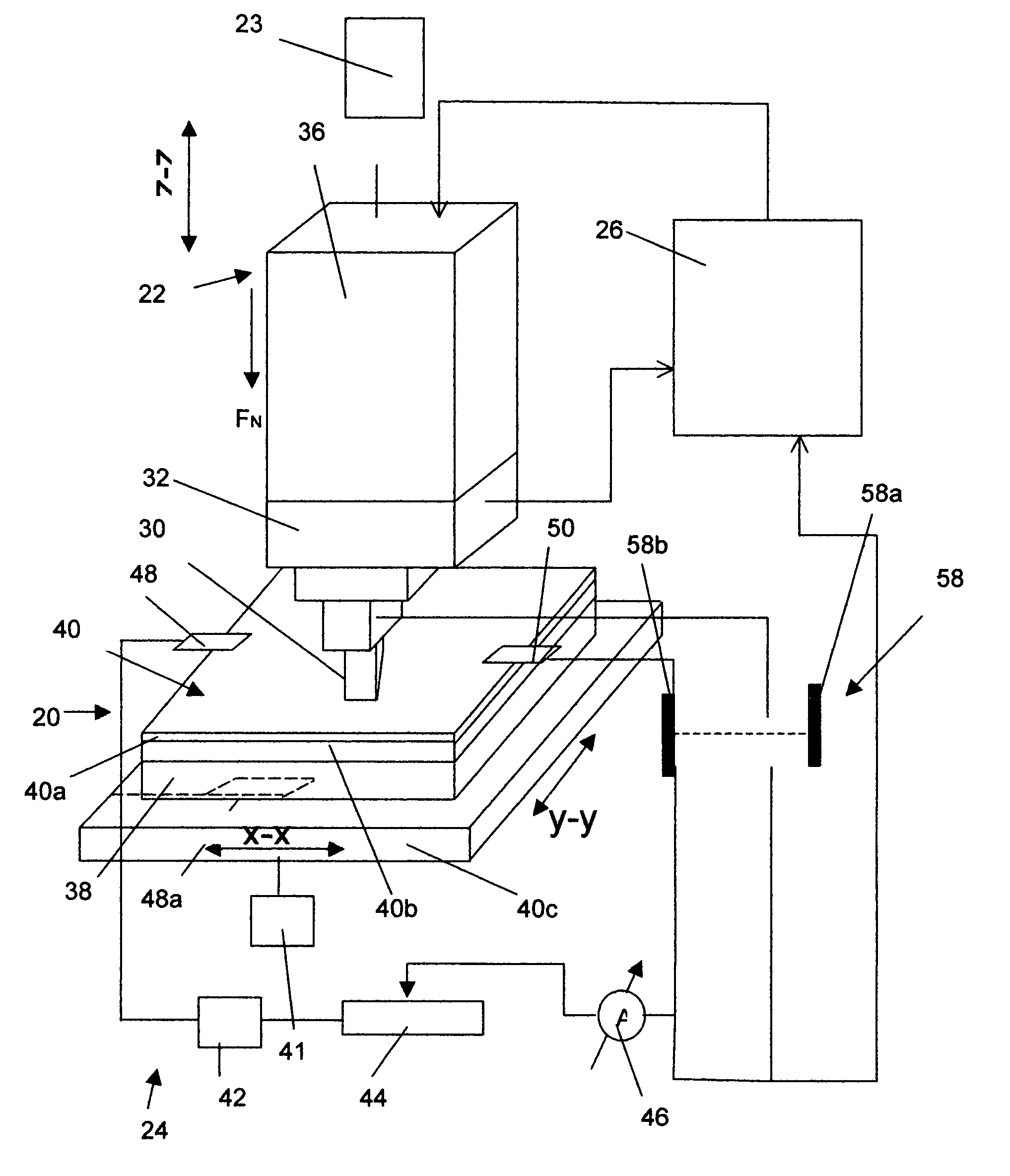
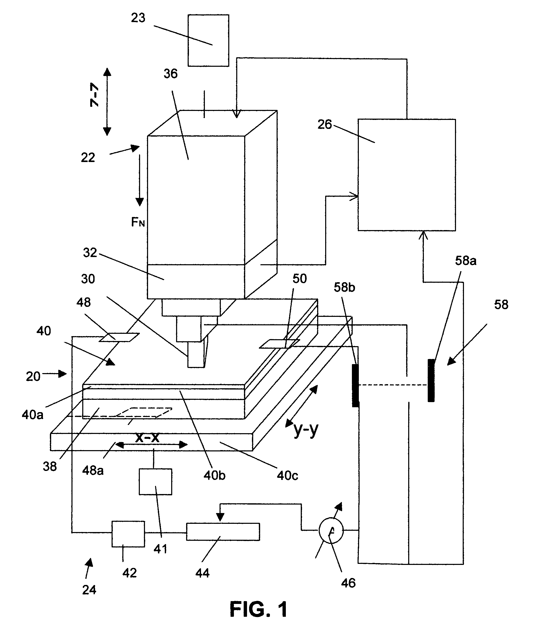
[0054] The tests were carried on objects 40 comprising liquid crystal display (LCD) samples. The LCD samples had an ultra-thin conductive coating of 10-nm thickness on a con-conductive polymer under-layer; three types of coatings (of the same material but deposited with three different processes) have been tested (samples #1 to #3). Each LCD sample was cut into 10×50 mm test specimens and clamped between the electrical contacts 48 and 50 (FIG. 1). A constant force was applied from the loading unit 36 via a closed-loop feedback servo control from the control unit 26. Two series of tests were performed, scratch tests as shown in FIG. 7 and wear tests as shown in FIG. 8.

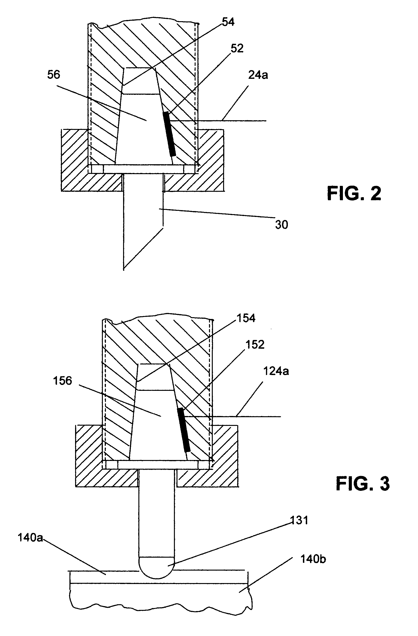
[0055] In the scratch tests, the indenter 30a was a standard Rockwell-C diamond indenter making unidirectional linear motion as illustrated in FIG. 7. A series of runs with progressively increasing force, though constant within each run, was performed in each test. The for...


PUM

PropertyMeasurementUnit
forceaaaaaaaaaa
forceaaaaaaaaaa
forceaaaaaaaaaa

Abstract

A method and apparatus of the invention are intended for determining characteristics of thin films, layers and coatings on under-layers and substrates when the films, layers and coatings have electrical characteristics measurably different from those of the under-layers and substrates. The method consists of selecting an object with an appropriate combination of a coating and substrate having different electrical characteristics, connecting one electrical contact to either the coating when the coating is more conductive than its substrate or to the substrate when the coating is less conductive than its substrate, connecting a second electrical contact to either the coating when the coating is conductive or to a conductive indenter when the coating is non-conductive, causing a relative movement between the indenter and the coating with application of an either constant or increasing force with simultaneous monitoring of electrical characteristics of the aforementioned circuit, until these characteristics change substantially and reach a critical level. The substantial changes in the electrical characteristics correspond to film or coating removal and exposure of the under-layer or substrate to the indenter. The characteristics of the thin films, layers and coatings are evaluated based on either critical load or distance or number of cycles corresponding to the substantial change in the electrical characteristics. The invention also relates to an apparatus for realization of the method.

Description

FIELD OF INVENTION [0001] The present invention relates to determining characteristics of films and coatings on under-layers or substrates. In particular, the invention relates to a method of testing durability characteristics of the aforementioned films and coatings via micro-scratching the surface of the films and coating by means of an indenter, which may be included into an electric measurement circuit. The invention also relates to the aforementioned tests based on deterioration of the film or coating by impressing an indenter under an applied force. The invention may find use for studying and testing durability and fatigue, wear and scratch resistance, adhesion and delamination resistance of conductive and non-conductive solid surfaces, coatings and films, as well as near-surface layers of various materials, including metals, composites, polymers, ceramics, etc. BACKGROUND OF THE INVENTION [0002] The use of coating films, both thin and thick, in various industries is increasin...

Claims


Application Information

Patent Timeline
Patent Type & Authority Applications(United States)
IPC IPC(8): G01N3/00G01N3/02G01N3/06G01N3/46
CPCG01N3/46G01N3/56G01N2203/0073G01N2203/0617G01N2203/0254G01N2203/0282G01N2203/0286G01N2203/0078
Inventor GITIS, NORM V.VINOGRADOV-NURENBERG, MICHAELXIAO, JUN
Owner NEVMET CORP
Learn More