Surface acoustic wave device
a surface acoustic wave and waveguide technology, applied in the field of surface acoustic waveguides, can solve the problems of filter transmission characteristics subject to spurious emission, deterioration of transmission/reception isolation characteristics, risk of an increase in chip size, etc., and achieve the effect of increasing chip size and greater miniaturization
- Summary
- Abstract
- Description
- Claims
- Application Information
AI Technical Summary
Benefits of technology
Problems solved by technology
Method used
Image
Examples
first embodiment
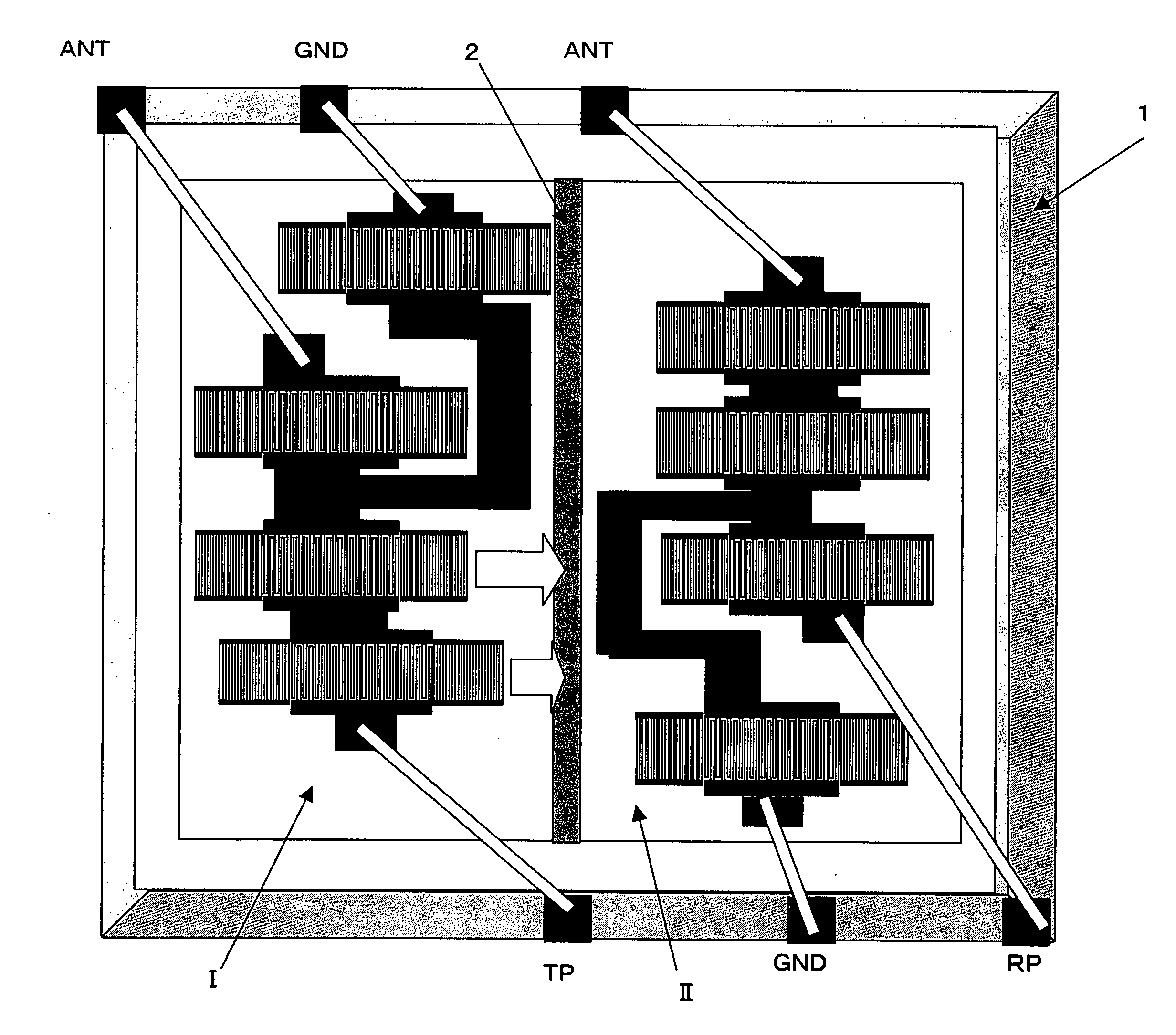
[0047] Therefore, the present invention resolves the problems of conventional methods of preventing the formation of short-circuiting of a surface acoustic wave. FIG. 5 is a surface acoustic wave device to which the present invention is applied.
[0048] A pair of SAW resonators 11 and 12 is formed opposite one another by means of a metallic film such as aluminum or an aluminum alloy on the surface of a piezoelectric substrate 10 of LiTaO3, LiNbO3, or the like. In addition, a metallic film 4 is formed between the SAW resonators 11 and 12.
[0049] The SAW resonators 11 and 12 each have a different frequency characteristic in the surface acoustic wave device that corresponds with the intended usage of the surface acoustic wave device. In addition, the positions in which the SAW resonators 11 and 12 are formed on the piezoelectric substrate 10 are in an at least partially overlapping relationship in a surface acoustic wave propagation region that is defined by virtually extending the respe...
third embodiment
[0058]FIG. 7 is the present invention in which an overlap surface acoustic wave propagation region is divided into two regions and the phases of surface acoustic waves are afforded an antiphase relationship to each other in the upper-half region and lower-half region of each of these divided regions.
[0059] In FIG. 7, the same reference numerals have been assigned to the same constituent elements as those of the above embodiment. As per the embodiment in FIG. 6, the resonators 11 and 12 are placed on a piezoelectric substrate 10. In addition, a metallic film 41 of width M / 2 and length L, which is disposed between the SAW resonators 11 and 12 of the embodiment in FIG. 6, is further divided into metallic films 411 and 412 of width M / 4.
[0060] As a result of this constitution, two metallic films 411 and 412 of width M / 4 and length L exist between the SAW resonators 11 and 12, and the surface acoustic wave 5 propagated by the SAW resonator 11 is separated into surface acoustic waves SAW-...
PUM
 Abstract
Description
Claims
Application Information
 - R&D
- Intellectual Property
- Life Sciences
- Materials
- Tech Scout
- Unparalleled Data Quality
- Higher Quality Content
- 60% Fewer Hallucinations
Browse by: Latest US Patents, China's latest patents, Technical Efficacy Thesaurus, Application Domain, Technology Topic, Popular Technical Reports.
© 2025 PatSnap. All rights reserved.Legal|Privacy policy|Modern Slavery Act Transparency Statement|Sitemap|About US| Contact US: help@patsnap.com


