
High frequency amplifier circuit permitting variable gain control

a variable gain control and amplifier technology, applied in amplifier modifications to reduce non-linear distortion, power management, wireless communication, etc., can solve the problem of deterioration of the high frequency characteristic, negative effect on the linearity of the attenuator, and the noise figure (nf), which is the ratio between the input sn ratio and the output sn ratio

Inactive Publication Date: 2005-06-02
FUJITSU LTD
View PDF8 Cites 52 Cited by
  • Summary
  • Abstract
  • Description
  • Claims
  • Application Information

AI Technical Summary

Benefits of technology

The present invention provides an amplifier circuit and a variable attenuator that have a small noise figure degradation with respect to a high frequency signal and a linear variable gain characteristic. The amplifier circuit includes an input terminal, an amplifier transistor, and a variable attenuator. The variable attenuator has a linear attenuation characteristic and includes a plurality of attenuation units in which an attenuation capacitor and a switch transistor are serially connected. The attenuation ratio is variably controlled by controlling the conduction of the switch transistor. The invention provides an amplifier circuit with improved high frequency performance.

Problems solved by technology

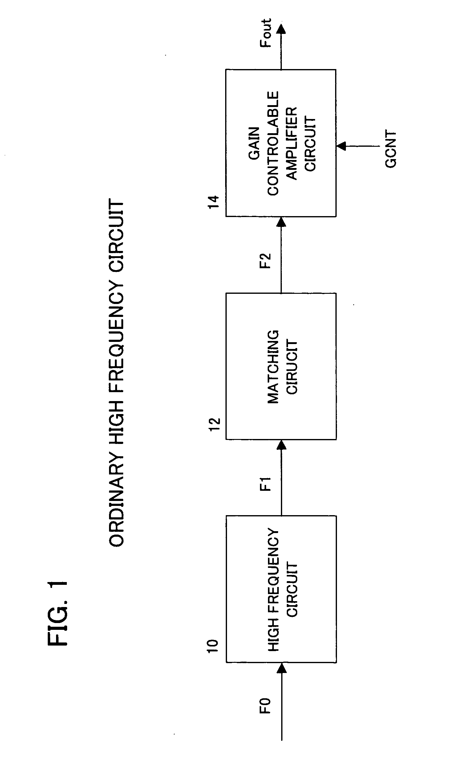
However, when the amplifier circuit shown in FIG. 2 is used in a low frequency band, the resistive elements of the pie-shaped attenuation circuits become a source of noise for the high frequency signal F2 in a high frequency band, such as 2 to 40 GHz, for example, and hence the noise figure (NF), which is the ratio between the input SN ratio and output SN ratio, deteriorates.
However, a parasitic capacitance between the silicon substrate and the impurity region affects high frequency signals, which brings about degradation of the high frequency characteristic.
In addition, switches SW1 and SW12 are provided in the transmission channel of the high frequency signal and therefore the characteristics of the transistor constituting these switches possess process dependency and so forth, which has an adverse effect on the linearity of the attenuator.

Method used


Image

  • High frequency amplifier circuit permitting variable gain control
  • High frequency amplifier circuit permitting variable gain control
  • High frequency amplifier circuit permitting variable gain control

Examples


Embodiment Construction

[0023] An embodiment of the present invention will be described hereinbelow with reference to the drawings. However, the technical scope of the present invention is not limited to or by this embodiment and is intended to cover the items appearing in the claims as well as any equivalents thereof.

[0024]FIG. 3 is a circuit diagram of the amplifier circuit of this embodiment. In this amplifier circuit, a variable attenuator 24 is provided upstream of an amplifier transistor unit 18. The constitution of the amplifier transistor unit 18 is the same as the example in FIG. 2 and therefore the same reference numbers have been assigned. This amplifier circuit is constituted by MOS transistors Q30, Q31, capacitive element Cout, resistive element R1, R2, and inductance element L, and so forth, which are provided on a silicon substrate.

[0025] The amplifier transistor unit 18 is provided with an N-channel transistor Q30 whose gate is supplied with the high frequency input signal F2 from the inp...


PUM


Abstract

The present invention is an amplifier circuit that permits variable gain control, comprising an input terminal to which a high frequency input signal is supplied; an amplifier transistor to the gate of which the high frequency input signal supplied to the input terminal is supplied and which generates an amplified signal at the drain side; and a variable attenuator provided in a signal transmission line between the input terminal and the gate of the amplifier transistor, in which a plurality of attenuation units in which an attenuation capacitor and a switch transistor are serially connected are provided in parallel between the signal transmission line and a power supply, and the attenuation ratio of which is variably controlled by controlling the conduction of the switch transistor.

Description

BACKGROUND OF THE INVENTION [0001] 1. Field of the Invention [0002] The present invention relates to a high frequency amplifier circuit that permits variable gain control, and, more particularly, a high frequency amplifier circuit that prevents noise figure degradation while retaining gain linearity and allows the number of elements to be reduced. [0003] 2. Description of the Related Art [0004] The implementation of a high frequency circuit by means of a silicon or compound semiconductor chip has been proposed. More particularly, as cellular phones, portable information terminals, and so forth, have become widespread, the development of low-cost silicon chips mounted with high frequency circuits that can be employed in microwave bands such as 2 to 40 GHz, for example, has progressed. [0005] Variable gain power amplifiers are employed in various places in high frequency circuits. However, in order to implement such a power amplifier in a silicon chip, the need for noise figure (NF) d...

Claims


Application Information

Patent Timeline
Patent Type & Authority Applications(United States)
IPC IPC(8): H03F1/32H03G1/00H03G3/10H03H11/24H04B7/005
CPCH04W52/52H03G1/0088
Inventor ARAI, TOMOYUKIENRIGHT, DAVID
Owner FUJITSU LTD
Learn More