
In plane switching mode liquid crystal display device and fabrication method thereof

Active Publication Date: 2005-05-05
LG DISPLAY CO LTD
View PDF2 Cites 27 Cited by
  • Summary
  • Abstract
  • Description
  • Claims
  • Application Information

AI Technical Summary

Benefits of technology

[0016] An advantage of the present invention is to provide an IPS mode LCD device capable of improving brightness of a screen by constructing red (R), green (G), blue (B) and white (W) sub-pixels as one unit pixel.
[0017] Another advantage of the present invention is to provide an IPS mode LCD device capable of effectively improving an aperture ratio by disposing four sub-pixels of red, green, blue and white in a quad-type (2×2 arrangement).
[0018] Yet another advantage of the present invention is to provide an IPS mode LCD device capable of easily controlling an area of sub-pixels by disposing a common line between sub-pixels that are disposed vertically, wherein the two sub-pixels share the common line
[0019] In order to achieve these and other advantages of the invention, an in plane switching mode liquid crystal display device comprises a first substrate and a second substrate; a plurality of gate lines disposed horizontally on the first substrate; a plurality of data lines disposed vertically on the first substrate, the plurality of gate lines and the plurality of data lines defining a first sub-pixel, a second sub-pixel, a third sub-pixel, and a fourth sub-pixel, wherein the sub-pixels are arranged in a 2×2 matrix form; at least one pair of first and second electrodes disposed in each sub-pixel; a first common line between the first and the second sub-pixels according to a first sub-pixel area ratio, the first common line connected to the first electrode disposed in the first and second sub-pixels; a second common line between the third and the fourth sub-pixels according to a second sub-pixel area ratio, the second sub-pixel area ratio being different from the first sub-pixel area ratio, and the second common line connected to the first electrode disposed in the third and fourth sub-pixels; a switching device formed at a crossing of the gate line and the data line; and a liquid crystal layer formed between the first and the second substrates.
[0020] In order to achieve these and other advantages of the invention, an in plane switching mode liquid crystal display device comprises a first substrate and a second substrate; a plurality of gate lines disposed horizontally on the first substrate; a plurality of data lines disposed vertically on the first substrate; a Red (R) sub-pixel, a Green (G) sub-pixel, a Blue (B) sub-pixel, and a White (W) sub-pixel defined by the gate lines and the data lines, wherein the sub-pixels are arranged in a 2×2 matrix form; at least one pair of a common electrode and a pixel electrode disposed in each sub-pixel; a first common line between the Red (R) and Green (G) sub-pixels according to a first area ratio, the first common line connected to the common electrode disposed in the Red (R) and Green (G) sub-pixels; a second common line between the Blue (B) and White (W) sub-pixels according to a second area ratio (B / W), the second area ratio being greater than 1, the second common line connected to the common electrode disposed in the Blue (B) and White (W) sub-pixels; a pixel electrode line overlapping the first and second common lines, forming a storage capacitor together with the first and second common lines, and electrically connecting the pixel electrode disposed in each sub-pixel; a switching device formed at a crossing of the gate line and the data line; and a liquid crystal layer formed between the first and the second substrates.
[0021] In order to achieve these and other advantages of the invention, a method of fabricating an in plane switching mode liquid crystal display device comprises providing a first substrate and a second substrate; forming a plurality of gate lines, a common electrode, and a common line on the first substrate, wherein the common line includes first and second common lines, the first common line disposed substantially at a center between the gate lines, the second common line disposed off-center between the gate lines, wherein the first and second common lines are electrically connected; forming a plurality of data lines disposed substantially perpendicularly to the gate lines and defining four sub-pixels together with the gate line and the first and the second common lines; a pixel electrode line overlapping the first and second common lines and forming a storage capacitor; and a pixel electrode substantially parallel to the common line and electrically connected to the pixel electrode line; and forming a liquid crystal layer between the first and second substrates.

Problems solved by technology

A twisted nematic (TN) mode liquid crystal display (LCD) device, which is commonly used as a flat panel display device achieving high image quality and low power consumption, has a problem in that its viewing angle is narrow because of refractive anisotropy of its liquid crystal molecules.
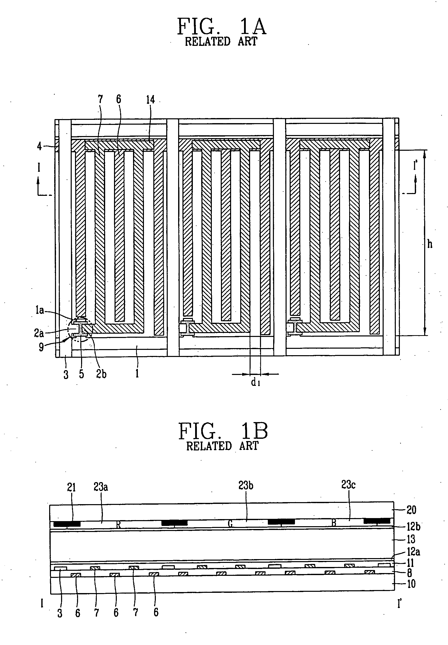
However, the related art IPS mode LCD device has problems in that an aperture ratio is decreased, and its brightness is degraded because the common electrode 6 and the pixel electrode 7 are disposed in a pixel region where light would otherwise be transmitted to form an image.

Method used


Image

  • In plane switching mode liquid crystal display device and fabrication method thereof
  • In plane switching mode liquid crystal display device and fabrication method thereof
  • In plane switching mode liquid crystal display device and fabrication method thereof

Examples


first embodiment

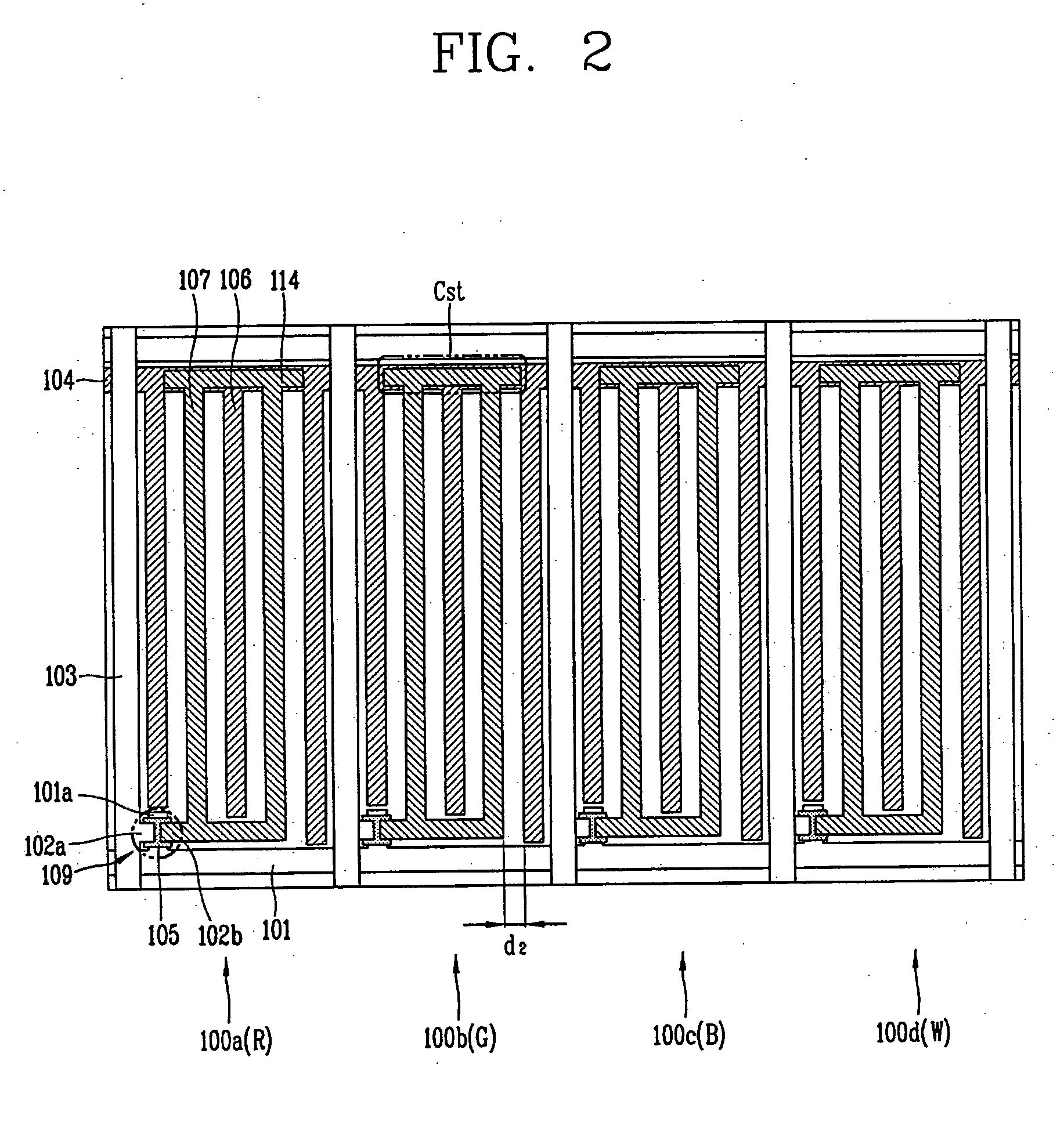
[0033]FIG. 2 illustrates the present invention: an in plane switching (IPS) mode liquid crystal display (LCD) device having a four transmissive regions within each sub-pixel. This embodiment of the IPS mode LCD device has a white(W) sub-pixel 100d in addition to the Red(R), Green(G) and Blue(B) sub-pixels (100a-100c). Here, the W sub-pixel 100d may be accommodated by reducing the width of each sub-pixel and maintaining the transmissive area of each sub-pixel.

[0034] The sub-pixels 100a, 100b, 100c and 100d are defined by a gate line 101 and a data line 103 arranged horizontally and vertically. In each sub-pixel 100a, 100b, 100c, 100d, a pixel electrode 107 substantially perpendicularly connects to a pixel electrode line 114, and a common electrode 106 perpendicularly connects to a common line 104. The pixel electrode 107 and the common electrode 106, which are alternately disposed, generate an in-plane electric field in the pixel when a voltage is applied between them. In addition, t...

second embodiment

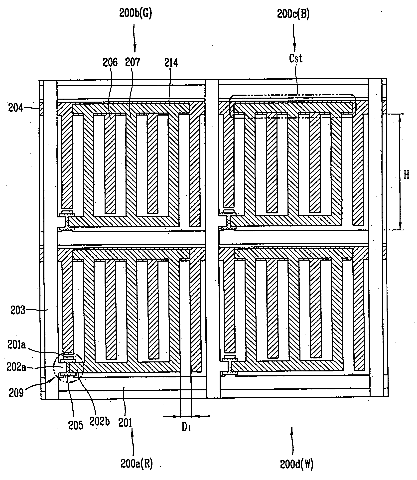
[0038] As illustrated in FIG. 3, the IPS mode LCD device has R, G, B and W sub-pixels 200a-200d, each having six transmissive regions, wherein the sub-pixels are arranged in the 2×2 matrix to form a unit pixel (P). The sub-pixels 200a-200d are defined by gate lines 201 and data lines 203, respectively, and are arranged horizontally and vertically. In each sub-pixel 200a-200d is at least one pair of electrodes, a pair including a pixel electrode 207 connected to the pixel electrode line 214, and a common electrode 206 connected to the common line 204. The pixel electrodes 207 may be substantially perpendicularly oriented relative to the pixel electrode line 214, and the common electrode 206 may be substantially perpendicularly oriented relative to the common line 204. The pixel electrodes 207 and the common electrodes 206 may be alternately disposed and generate an in-plane electric field in the pixel on the application of a voltage. Further, the pixel electrode line 214 may overlap...

third embodiment

[0043] As illustrated in FIG. 4, in the IPS mode LCD device a unit pixel is divided into sub-pixels by a common line 304 passing substantially through a center of the pixel (P) parallel to a gate line 301, and R, G, B and W sub-pixels 300a-300d are arranged in a 2×2 matrix form. The region above the common line 304 may be referred to as a first region, and the region below the common line 304 may be referred to as a second region. As illustrated in FIG. 4, the G and B sub-pixels 300b and 300c are disposed in the first region, and R and W sub-pixels 300a and 300d are disposed in the second region. It will be apparent that this exemplary embodiment may have the R, G, B, and W sub-pixels arranged in other configurations than that shown in FIG. 4.

[0044] The common line 304 is electrically connected to at least one common electrode 306 disposed in each sub-pixel, and forms a storage capacitor (Cst) together with a pixel electrode line 314 overlapping the common line 304. As illustrated ...


PUM


Abstract

An in plane switching mode liquid crystal display device and its fabrication method are disclosed. The in plane switching mode liquid crystal display device includes: a first and second substrate; a gate line and a data line respectively disposed horizontally and vertically on the first substrate; a first to a fourth sub-pixels defined by the gate line and the data line and arranged in a 2×2 matrix form; at least one pair of first and second electrodes disposed in each sub-pixel and generating an in-plane electric field; a first common line equally dividing the first and the second sub-pixels and connected to the first electrode disposed in the first and the second sub-pixels; a second common line dividing the third and the fourth sub-pixels to make an area of one of said sub-pixels larger than the other one and connected to the first electrode disposed in the third and the fourth sub-pixels; a switching device formed at a crossing of the gate line and the data line; and a liquid crystal layer formed between the first and the second substrates.

Description

[0001] This application claims the benefit of Korean Patent Application No. 76079 / 2003 filed on Oct. 29, 2003, which is hereby incorporated by reference for all purposes as if fully set forth herein. BACKGROUND OF THE INVENTION [0002] 1. Field of the Invention [0003] The present invention relates to a liquid crystal display device, and particularly to an in plane switching mode liquid crystal display device and its fabrication method capable of easily controlling areas of red, green, blue and white sub-pixels arranged in a 2×2 matrix form. [0004] 2. Description of the Related Art [0005] A twisted nematic (TN) mode liquid crystal display (LCD) device, which is commonly used as a flat panel display device achieving high image quality and low power consumption, has a problem in that its viewing angle is narrow because of refractive anisotropy of its liquid crystal molecules. This is because liquid crystal molecules are aligned parallel to a substrate in the absence of a voltage and are...

Claims


Application Information

Patent Timeline
IPC IPC(8): G02F1/133G02F1/1368G02F1/1343G02F1/136G02F1/1362H01L21/00H01L29/786
CPCG02F1/134363G02F2201/52G02F1/136213G02F1/1343
Inventor BAEK, HEUME-LL
Owner LG DISPLAY CO LTD
Learn More