
Barrier layer including a titanium nitride liner for a copper metallization layer including a low-k dielectric

a technology of metallization layer and titanium nitride, which is applied in the direction of semiconductor devices, electrical apparatus, semiconductor/solid-state device details, etc., can solve the problems of inefficient application of copper on a substrate in large amounts, affecting the wettability and coverage affecting the wettability of copper metallization layers, etc., to achieve the effect of superior wettability and coverage and high throughpu

Inactive Publication Date: 2005-05-05
ADVANCED MICRO DEVICES INC
View PDF4 Cites 14 Cited by
  • Summary
  • Abstract
  • Description
  • Claims
  • Application Information

AI Technical Summary

Benefits of technology

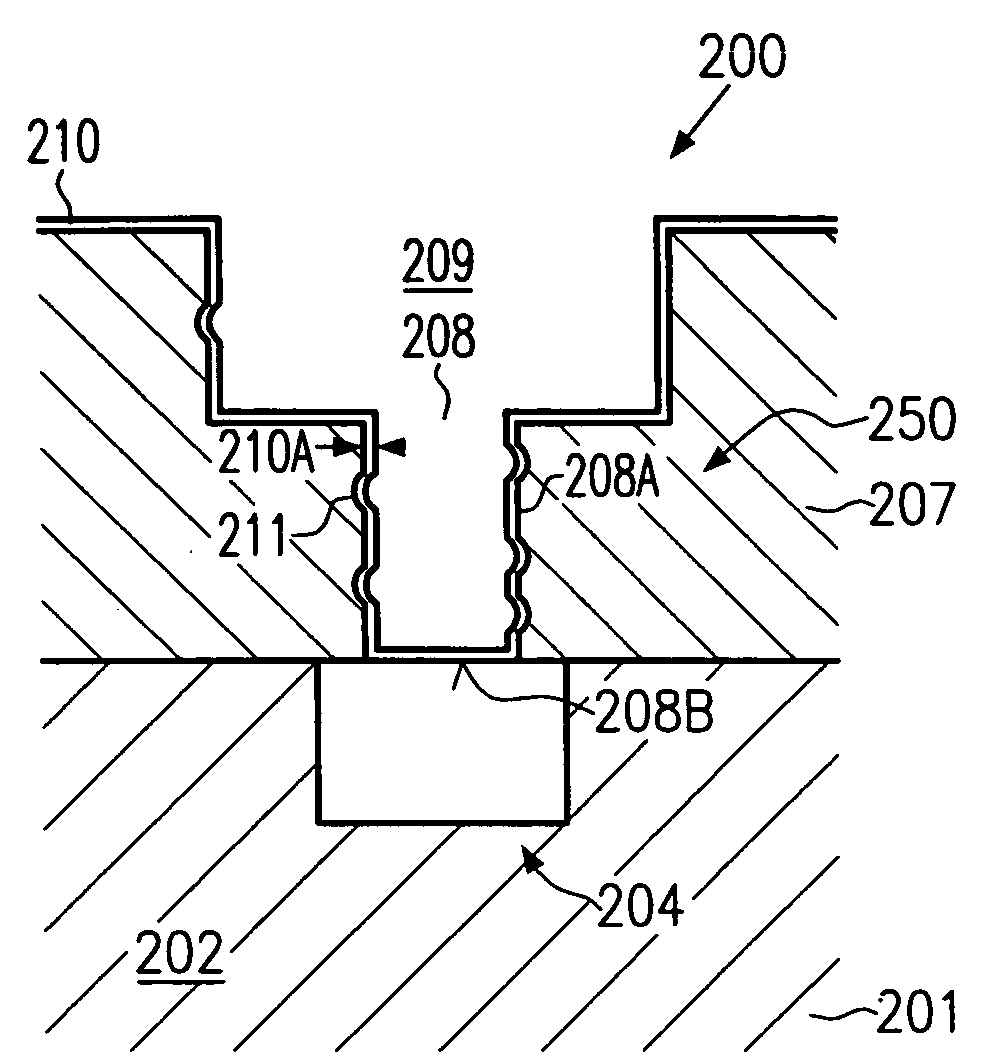
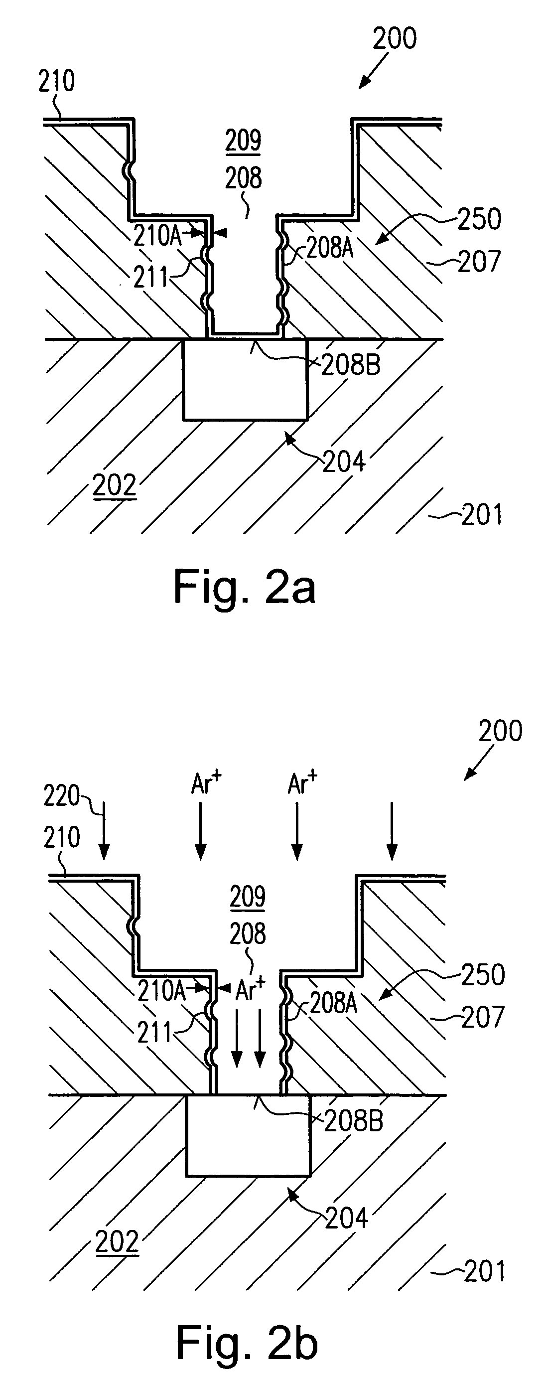
The present invention provides a technique for forming a conductive barrier layer for an interconnect feature that provides superior wettability and coverage for a subsequently deposited metal, while at the same time assuring high throughput in that currently available deposition tools may effectively be utilized. This is achieved by depositing a thin titanium nitride liner that reliably covers sidewalls of vias and trenches, even in low-k materials and porous materials, which then serves as an efficient wetting layer for a subsequent material. The invention also provides semiconductor structures and methods for forming interconnect features with improved barrier layers for better performance and reliability.

Problems solved by technology

Due to the large number of circuit elements and the required complex layout of the integrated circuits, generally, the electrical connection of the individual circuit elements may not be established within the same level on which the circuit elements are manufactured, but requires one or more additional “wiring” layers, also referred to as metallization layers.
The fabrication of a plurality of metallization layers entails extremely challenging issues to be solved, such as mechanical, thermal and electrical reliability of up to twelve stacked metallization layers that may be employed on sophisticated aluminum-based microprocessors.
Despite these advantages, copper also exhibits a number of disadvantages regarding the processing and handling of copper in a semiconductor facility.
For instance, copper may not be efficiently applied onto a substrate in larger amounts by well-established deposition methods, such as chemical vapor deposition (CVD), and also may not be effectively patterned by the usually employed anisotropic etch procedures.
A further major drawback to the use of copper is its propensity to readily diffuse in many dielectric materials such as silicon dioxide, which is a well-established and approved dielectric material in fabricating integrated circuits.
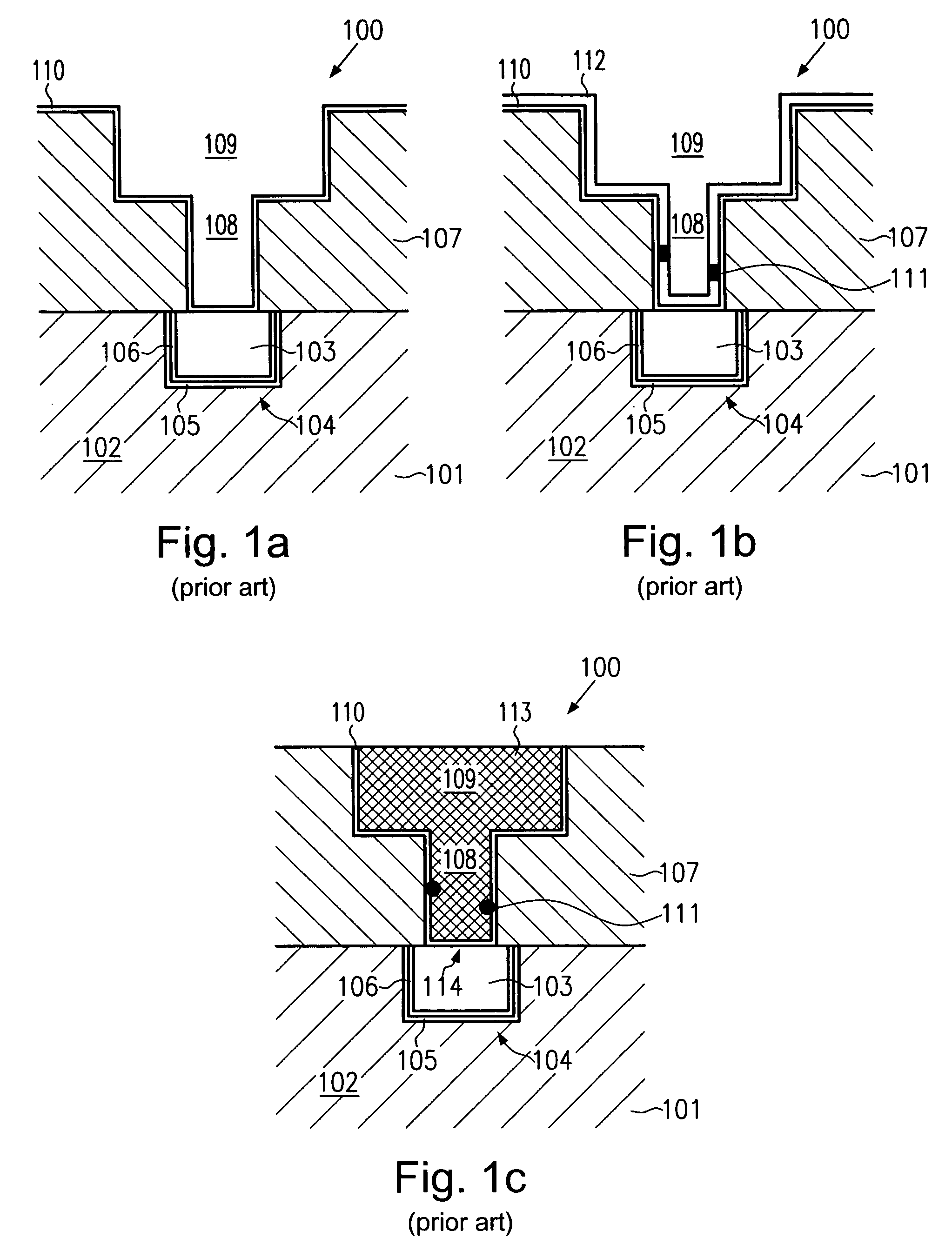
Hence, complex barrier technologies are required to support further device scaling, wherein the usage of low-k dielectric materials may even impart further increased constraints to the barrier layer, as will be described for a typical process technique for sophisticated copper-based integrated circuits with reference to FIGS. 1a-1c.
In highly advanced devices requiring a barrier layer thickness of approximately 10 mn or even less, these techniques may not readily provide the required sidewall coverage, especially due to the fact that many of the low-k dielectric materials used may have a porous structure, which may therefore lead to the formation of openings on the sidewalls of the via 108 and on the sidewalls and the bottom of the trench 109.
The advanced sputter techniques usually employed for tantalum-based barrier layers may therefore not be applied with the desired efficiency, since these techniques are highly directional in nature and may not provide the capability for efficiently filling voids at sidewalls of the via 108 without requiring an unduly overall layer thickness.
As a consequence, portions or defects 111 may result, for instance at critical locations within the via 108 having a reduced seed layer thickness, thereby adversely affecting the subsequent deposition of copper on the semiconductor structure 100 by, for example, electroplating.

Method used


Image

  • Barrier layer including a titanium nitride liner for a copper metallization layer including a low-k dielectric
  • Barrier layer including a titanium nitride liner for a copper metallization layer including a low-k dielectric
  • Barrier layer including a titanium nitride liner for a copper metallization layer including a low-k dielectric

Examples


Embodiment Construction

[0022] Illustrative embodiments of the invention are described below. In the interest of clarity, not all features of an actual implementation are described in this specification. It will of course be appreciated that in the development of any such actual embodiment, numerous implementation-specific decisions must be made to achieve the developers' specific goals, such as compliance with system-related and business-related constraints, which will vary from one implementation to another. Moreover, it will be appreciated that such a development effort might be complex and time-consuming, but would nevertheless be a routine undertaking for those of ordinary skill in the art having the benefit of this disclosure.

[0023] The present invention will now be described with reference to the attached figures. Although the various regions and structures of a semiconductor device are depicted in the drawings as having very precise, sharp configurations and profiles, those skilled in the art reco...


PUM

PropertyMeasurementUnit
relative permittivityaaaaaaaaaa
thicknessaaaaaaaaaa
thicknessaaaaaaaaaa

Abstract

An improved barrier technology for interconnect features, especially for copper-based interconnects, is provided. A thin titanium nitride liner is conformally deposited by chemical vapor deposition so as to reliably cover all inner surfaces of the interconnect features, even if formed within a porous material, and thus provides a surface area having improved wettability for the deposition of a subsequent barrier material. Hence, the step coverage of a sputter deposition technique, typically used for tantalum-based barrier layers, may be successfully used in combination with the titanium nitride liner, thereby improving the wetting properties for the subsequent copper seed deposition compared to a tantalum-based barrier layer formed by ALD. Moreover, the provision of a CVD titanium nitride liner in combination with a sputter deposited barrier layer assures a significantly higher throughput compared to the conventional atomic layer deposition approach.

Description

BACKGROUND OF THE INVENTION [0001] 1. Field of the Invention [0002] Generally, the present invention relates to the formation of integrated circuits, and, more particularly, to the formation of metallization layers including highly conductive metals, such as copper, embedded into a dielectric material having low permittivity to enhance device performance. [0003] 2. Description of the Related Art [0004] In an integrated circuit, a huge number of circuit elements, such as transistors, capacitors, resistors and the like, are formed in or on an appropriate substrate, usually in a substantially planar configuration. Due to the large number of circuit elements and the required complex layout of the integrated circuits, generally, the electrical connection of the individual circuit elements may not be established within the same level on which the circuit elements are manufactured, but requires one or more additional “wiring” layers, also referred to as metallization layers. These metalliz...

Claims


Application Information

Patent Timeline
Patent Type & Authority Applications(United States)
IPC IPC(8): H01L21/768H01L23/522H01L23/532
CPCH01L21/76843H01L21/76844H01L21/76865H01L23/5226H01L2924/0002H01L23/53238H01L2924/00
Inventor KAHLERT, VOLKERFRIEDEMANN, MICHAEL
Owner ADVANCED MICRO DEVICES INC
Learn More