Plasma chemical vapor deposition apparatus having an improved nozzle configuration

Inactive Publication Date: 2005-05-05
SAMSUNG ELECTRONICS CO LTD
View PDF4 Cites 29 Cited by
  • Summary
  • Abstract
  • Description
  • Claims
  • Application Information

AI Technical Summary

Benefits of technology

[0012] Exemplary embodiments of the present invention provide a plasma chemical vapor deposition apparatus including nozzles configured for reducing the excitation of sources gases within the nozzles and thereby suppressing or eliminating the formation of deposits on the inner walls of the nozzles. Exemplary embodiments of the present invention also provide a plasma chemical vapor deposition apparatus including both nozzles and injection pipes configured for producing a more uniform deposition across the entire surface of a wafer.
[0015] The gas injection part has at least one nozzle and at least one injection pipe. A plurality of nozzles are regularly arranged in the lower chamber to be directed into the upper chamber. Each of the nozzles includes a single channel portion in which a passage of the source gas mixture is formed and a compound channel portion in which one or more passages of the source gas mixture is formed. The single channel portion is connected to a gas supply assembly, and the compound channel portion extends from the single channel portion. The respective passages of the compound channel portion are configured to have a smaller width than the passage of the single channel portion, thereby reducing or suppressing reaction of the source gas mixture in the nozzle. In the compound channel portion, each of the passages has a width of, at most, about 2 millimeters.

Problems solved by technology

Because an accumulation of these deposits can separate from the inner surfaces and result in particulate contamination on subsequent substrates, conventional CVD deposition processes generally incorporate a regular periodic cleaning step to remove the depositions from the inner surfaces of the chamber.
However, as a result of the configuration of the nozzle, a cleaning process sufficient to remove such deposits from the nozzle will generally constitute a severe overetch of the remainder of the chamber surfaces.
The repeated overetching of the inner wall of the chamber will tend to shorten lifespan of the deposition apparatus, lower the operating ratio of the apparatus, increase the maintenance costs and reduce the wafer throughput and productivity of the apparatus.
This disparity in the source gas distribution increases the difficulty in achieving a substantially uniform deposition across the entire wafer surface during a deposition process.

Method used


Image

  • Plasma chemical vapor deposition apparatus having an improved nozzle configuration
  • Plasma chemical vapor deposition apparatus having an improved nozzle configuration
  • Plasma chemical vapor deposition apparatus having an improved nozzle configuration

Examples


Embodiment Construction

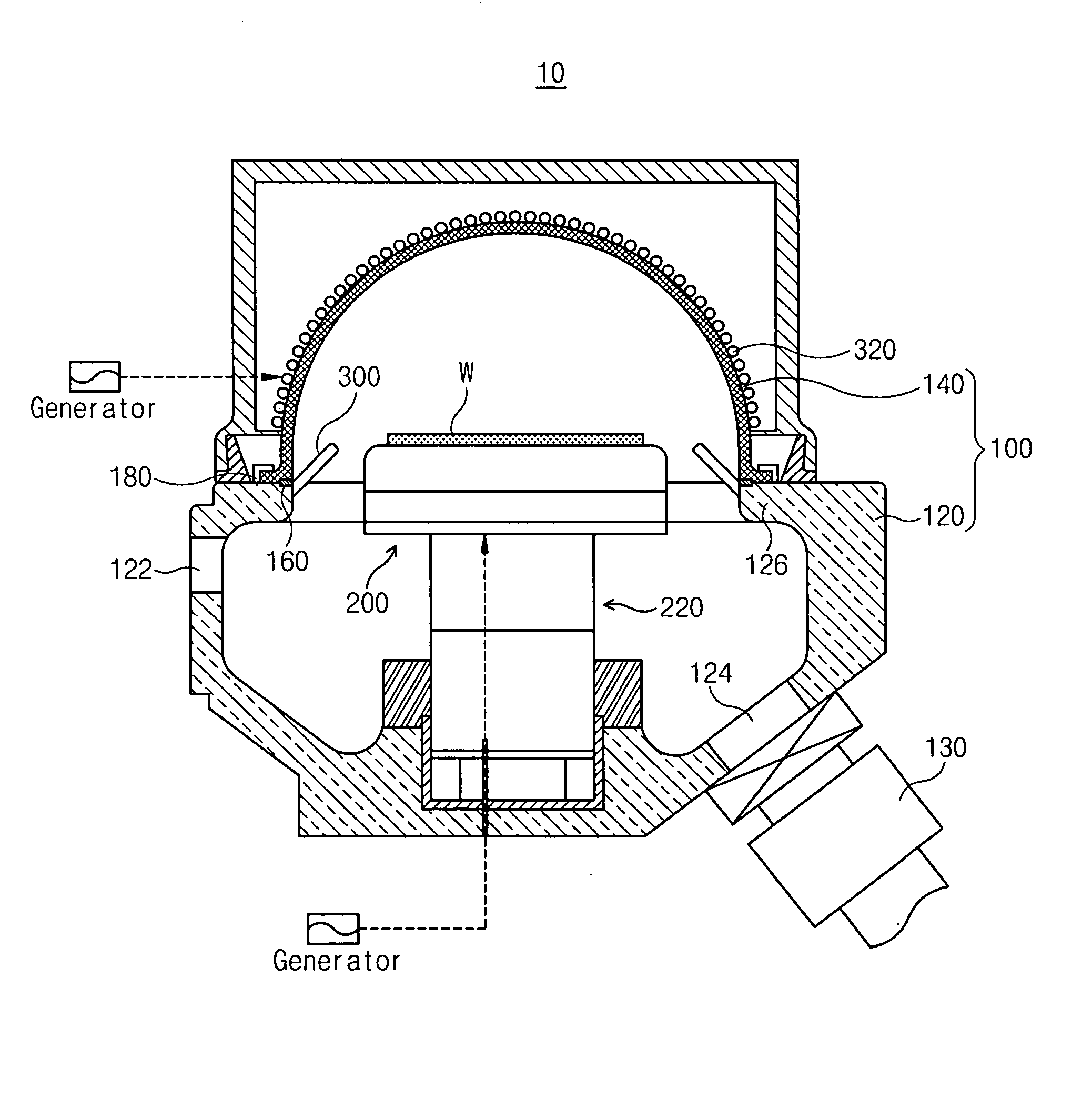
[0046] An exemplary high density plasma chemical vapor deposition (HDP-CVD) apparatus 10 according to the invention will now be described with reference to FIG. 1. As illustrated in FIG. 1, the HDP-CVD apparatus 10 includes a process chamber 100, a substrate supporter 200, a supporter driving part 220, an upper electrode 320, a lower electrode (not shown), and a gas injection part. The process chamber 100 provides a space in which deposition processes may be performed that may be sealed from the outside and maintained at pressures typically below atmospheric pressure.

[0047] As illustrated, the process chamber 100 includes both a lower chamber 120 and an upper chamber 140. An opening is provided in the upper portion of the lower chamber 120 for moving a wafer W into the upper chamber 140. One or more openings 122 may be provided in the sidewall of the lower chamber 120 for transferring wafers into and out of the lower chamber. An exhaust port 124 may be provided in a portion of the ...


PUM

PropertyMeasurementUnit
Lengthaaaaaaaaaa
Lengthaaaaaaaaaa
Timeaaaaaaaaaa

Abstract

Provided is a high density plasma chemical vapor deposition (HDP-CVD) apparatus that includes a plurality of nozzles and / or injection pipes arranged for injecting a source gas mixture into a reaction chamber. The nozzles will each include an outlet region that includes a plurality of outlet channels or ports, the outlet channels are, in turn, configured to have a sufficiently small width and a sufficient length to suppress the formation of a plasma within the source gases passing through the respective nozzles. By suppressing the formation of a plasma within the nozzles, the thickness of deposits formed on the nozzles during the deposition processes can be maintained at a level generally no greater than deposits formed on the other chamber surfaces. This control of the deposit thickness allows the nozzles to be cleaned effectively by the same cleaning process applied to the chamber.

Description

CROSS-REFERENCE TO RELATED APPLICATIONS [0001] This application claims priority from Korean Patent Application No. 2003-77396, which was filed on Nov. 3, 2003, and Korean Patent Application No. 2004-25097, which was filed on Apr. 12, 2004, in the Korean Intellectual Property Office, the disclosures of which are incorporated herein in their entirety by reference. BACKGROUND OF THE INVENTION [0002] 1. Field of the Invention [0003] The present invention relates to an apparatus used for manufacturing semiconductor devices and, more particularly, to a plasma chemical vapor deposition (“CVD”) apparatus for depositing a layer of a material on a semiconductor substrate using plasma and a nozzle configuration useful in such a plasma CVD apparatus. [0004] 2. Description of Related Art [0005] A significant deposition process utilized repeatedly during the manufacture of semiconductor devices is a chemical vapor deposition (CVD) process, which may be used to form or deposit a wide variety of fi...

Claims


Application Information

Patent Timeline
IPC IPC(8): C23C16/44C23C16/455C23C16/507H01J37/32H01L21/31
CPCC23C16/45512C23C16/45563H01J37/3244H01J37/321C23C16/507
Inventor MOON, AHN-SIKYANG, YUN-SIKHAN, JAE-HYUNHONG, JOO-PYOCHAE, SEUNG-KILEE, IN-CHEOLLEE, JONG-KOOKIM, DAE-HYUN
Owner SAMSUNG ELECTRONICS CO LTD
Why Eureka
Try Eureka