Eureka AIR delivers breakthrough ideas for toughest innovation challenges, trusted by R&D personnel around the world.

Group III-nitride on Si using epitaxial BP buffer layer

a buffer layer and nitride technology, applied in the direction of semiconductor devices, basic electric elements, electrical equipment, etc., can solve the problems of difficult to obtain gan bulk crystals, no readily available suitable substrate materials, expensive and only available in small wafer sizes

Inactive Publication Date: 2005-04-28
FLORIDA UNIV OF A FLORIDA +1
View PDF2 Cites 27 Cited by
  • Summary
  • Abstract
  • Description
  • Claims
  • Application Information

AI Technical Summary

Benefits of technology

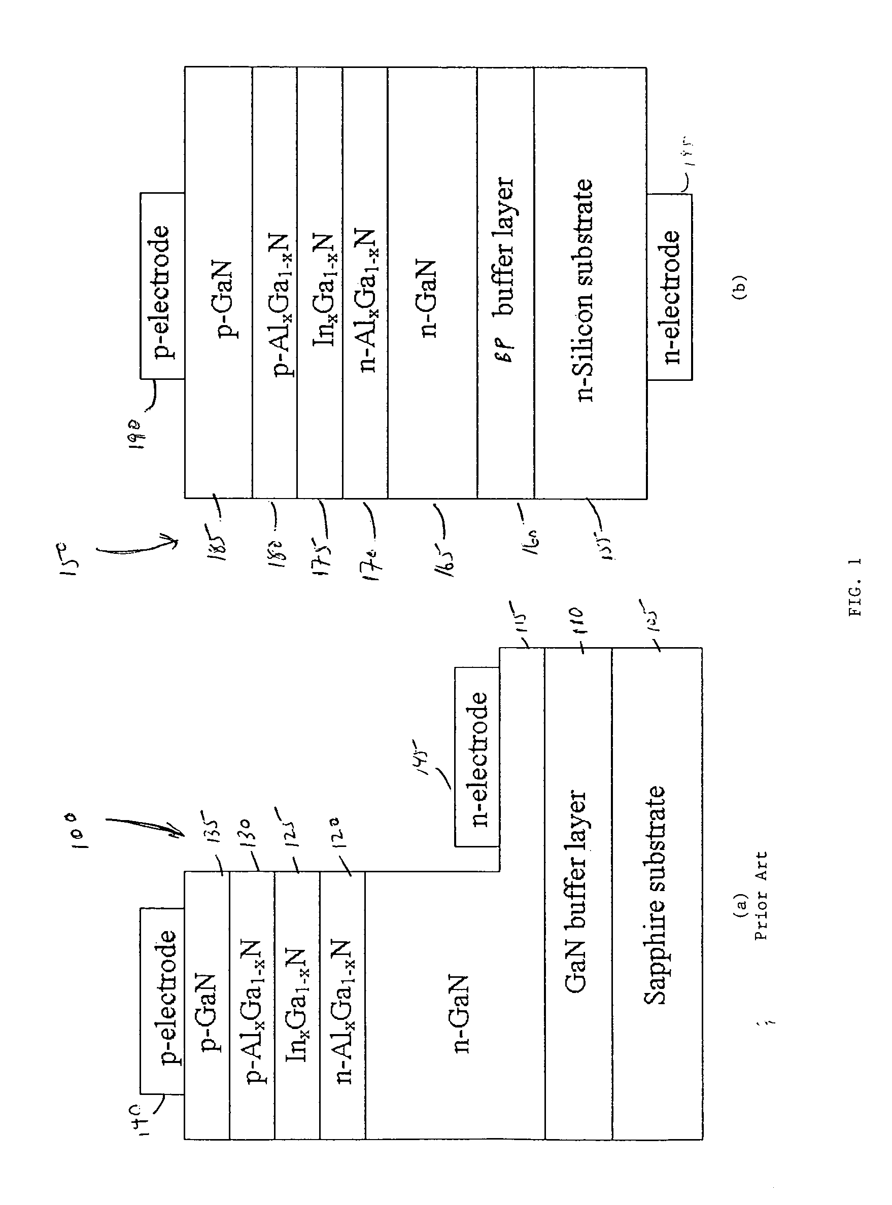
This patent describes a method for making semiconductor devices using a silicon substrate and a layer of epitaxial boron phosphide (BP) with a group III nitride semiconductor epitaxial layer on top. The BP layer is preferably single crystal and the group III nitride layer can be single crystal GaN. The method also includes steps for removing native oxide on the silicon substrate surface and depositing a second cladding layer. The technical effects of this patent include improved device performance and reliability, as well as more efficient and cost-effective manufacturing.

Problems solved by technology

Due to the high equilibrium pressure of nitrogen at typical growth temperatures, it is extremely difficult to obtain GaN bulk crystals.
However, a current problem with the manufacture of GaN thin films is that there is no readily available suitable substrate material which exhibits close lattice matching and close matching of thermal expansion coefficients.
SiC is a semiconducting material which provides excellent thermal conductivity, but is very expensive and available only in small wafer sizes.
Direct growth of GaN on SiC is generally difficult due to poor wetting between these materials.
In addition, it is very difficult to prepare a SiC layer having a smooth surface.
A rough interface with GaN can cause an increase in defect density of the GaN layer.
However, the lattice mismatch between GaN and sapphire is over 13%.
Such a huge mismatch in the lattice constants causes poor crystal quality if GaN films were to be grown directly on the sapphire, due to stress formation and a high density of defects, including such defects as microtwins, stacking faults and deep-levels.
Use of electrically insulating substrates can complicate processing by requiring additional processing steps, as compared to a conducting or semiconducting substrate, due to the inability to make an electrical contact through the substrate.
The disadvantages of Si as a substrate for GaN heteroepitaxy include a +20.5% a-plane misfit which initially led to the conclusion that growth of GaN directly on silicon was not likely to work well.
In addition, the thermal expansion misfit between GaN (5.6×10⁻⁶ K−1) and Si (6.2×10⁻⁶ K−1) of 9.6% can lead to cracking upon cooling in films grown at high temperature.
Moreover, GaN is also known to poorly nucleate on Si substrate, leading to an island-like GaN structure and poor surface morphology.
Thus, the quality of GaN films grown on silicon has been far inferior to that of films grown on other commonly used substrates such as sapphire or silicon carbide.
Moreover, the growth conditions that have been used for GaN on Si are generally not compatible with standard silicon processes.
However, even when buffer layers are used, typically the effect of the thermal expansion coefficient mismatch is too large to suppress the formation of cracks in the GaN and related other Group III-N films grown.

Method used


Image

  • Group III-nitride on Si using epitaxial BP buffer layer
  • Group III-nitride on Si using epitaxial BP buffer layer
  • Group III-nitride on Si using epitaxial BP buffer layer

Examples


example

[0034] It should be understood that the examples and embodiments described herein are for illustrative purposes only and that various modifications or changes in light thereof will be suggested to persons skilled in the art and are to be included within the spirit and purview of this application. The invention can take other specific forms without departing from the spirit or essential attributes thereof.

[0035] Commercial Si (111) substrates were provided. The Si substrates were first cleaned in warm trichloroethylene(TCE) / acetone / methanol and etched for one minute in dilute HF, such as 1% HF. The wafers were loaded into a reactor. Prior to BP growth, in-situ hydrogen reduction (e.g. 4% H2 in N2) was performed for ten minutes at or near the BP epitaxial growth temperature, such as at 1000° C. for an 1100° C. BP deposition process to remove the native oxide on the surface of the silicon substrate.

[0036] CVD of epitaxial BP on Si (111) was performed using boron trichloride (BCl3, 99...


PUM

PropertyMeasurementUnit
thicknessaaaaaaaaaa
sublimation temperatureaaaaaaaaaa
temperatureaaaaaaaaaa

Abstract

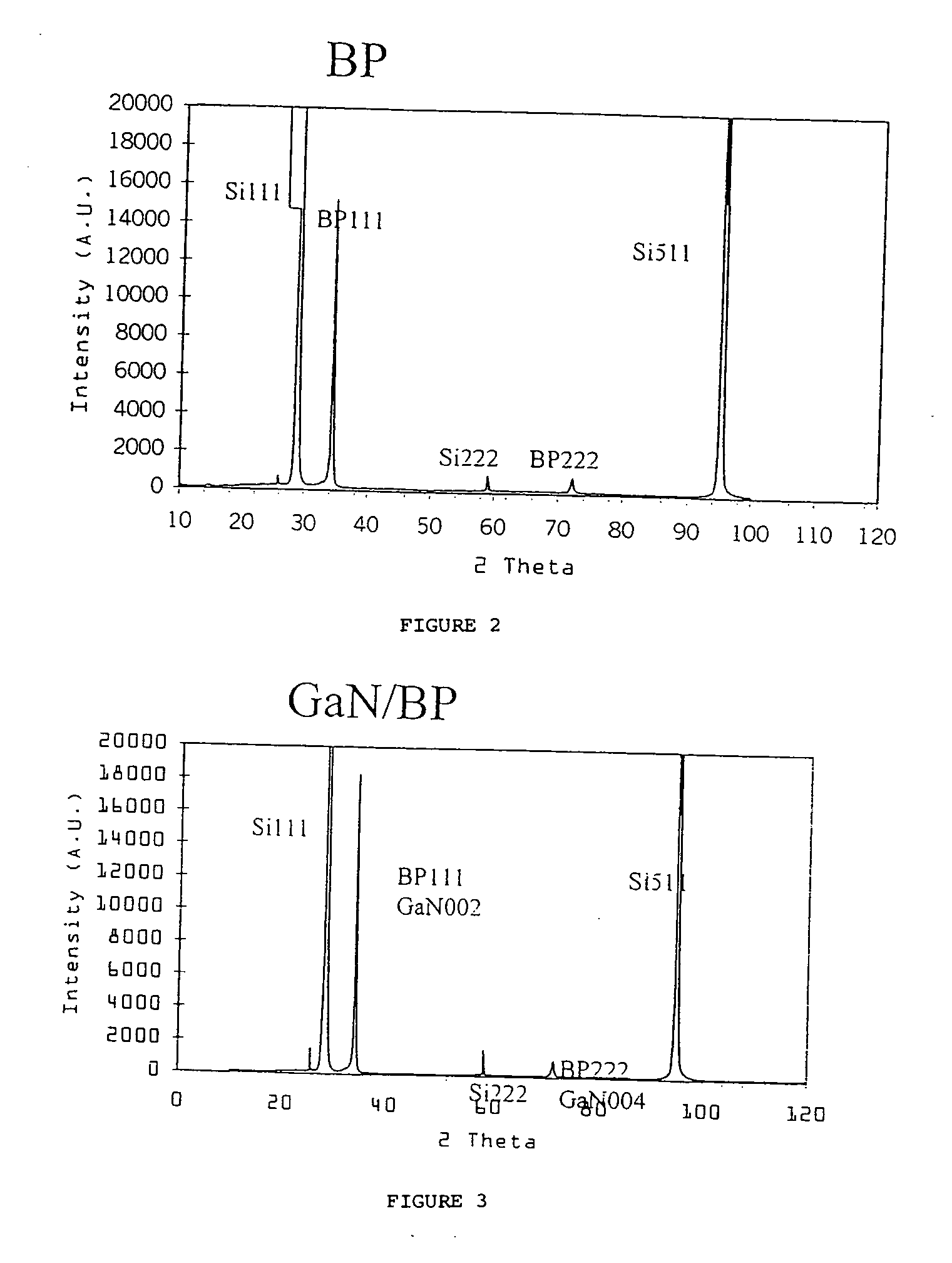
A semiconductor device and method for forming the same includes a silicon (111) single crystal substrate, and an epitaxial boron phosphide (BP) layer disposed on the substrate. A group III-nitride semiconductor epitaxial layer is disposed on the BP epitaxial layer.

Description

CROSS-REFERENCE TO RELATED APPLICATIONS [0001] Not applicable. STATEMENT REGARDING FEDERALLY SPONSORED RESEARCH OR DEVELOPMENT [0002] Not applicable. FIELD OF THE INVENTION [0003] The invention relates to the field of thin film based devices, and more specifically, to a method of improving the quality of Group III-N thin films which have poor lattice matching with the substrate onto which they are deposited, and related articles. BACKGROUND OF THE INVENTION [0004] Group III-N compounds, such as gallium nitride (GaN) and its related alloys have been under intense research in recent years due to their promising applications in electronic and optoelectronic devices. Particular examples of potential optoelectronic devices include blue light emitting and laser diodes, and UV photodetectors. Their large bandgap and high electron saturation velocity also make them excellent candidates for applications in high temperature and high-speed power electronics. [0005] Due to the high equilibrium ...

Claims


Application Information

Patent Timeline
Patent Type & Authority Applications(United States)
IPC IPC(8): H01L21/20H01L21/205H01L27/15H01L33/00H01L33/12
CPCH01L21/02381H01L21/02461H01L21/0254H01L33/12H01L21/02661H01L33/007H01L21/0262
Inventor KRYLIOUK, OLGAANDERSON, TIMBCHIR, OMAR J.KIM, KEE CHAN
Owner FLORIDA UNIV OF A FLORIDA
Why Eureka
Eureka Blog
Learn More