
Novel method to reduce Rs pattern dependence effect

Active Publication Date: 2005-04-21
TAIWAN SEMICON MFG CO LTD
View PDF11 Cites 42 Cited by
  • Summary
  • Abstract
  • Description
  • Claims
  • Application Information

AI Technical Summary

Benefits of technology

[0013] An objective of the present invention is to provide an improved method for fabricating copper wiring that produces a Rs value which is nearly independent of copper line width or pattern density.
[0014] A further objective of the present invention is to provide an improved method of forming copper wiring without dishing in order to prevent undesirably high Rs values that are common for wide interconnects.
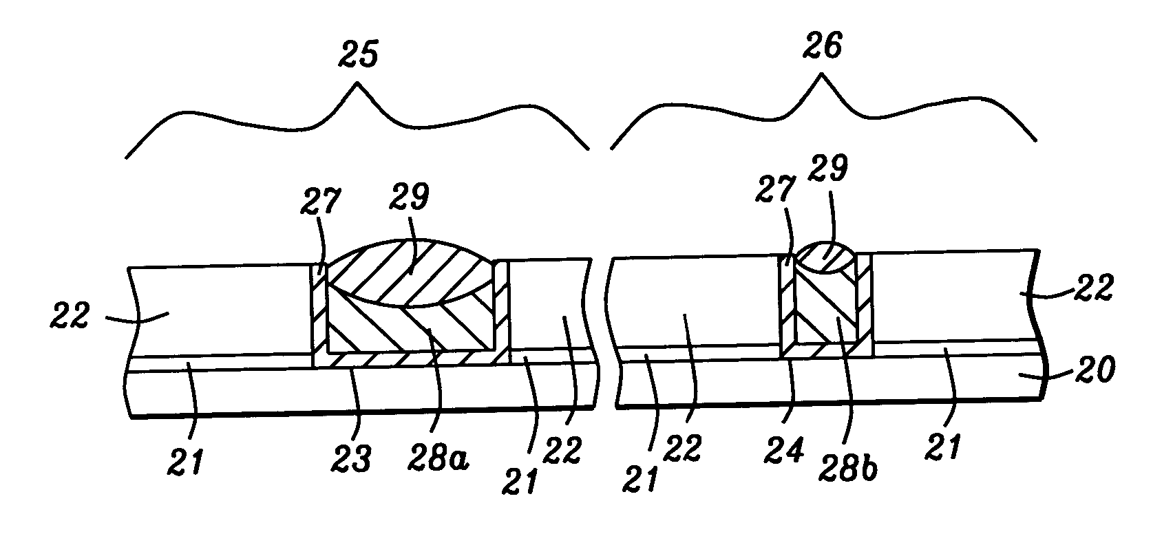
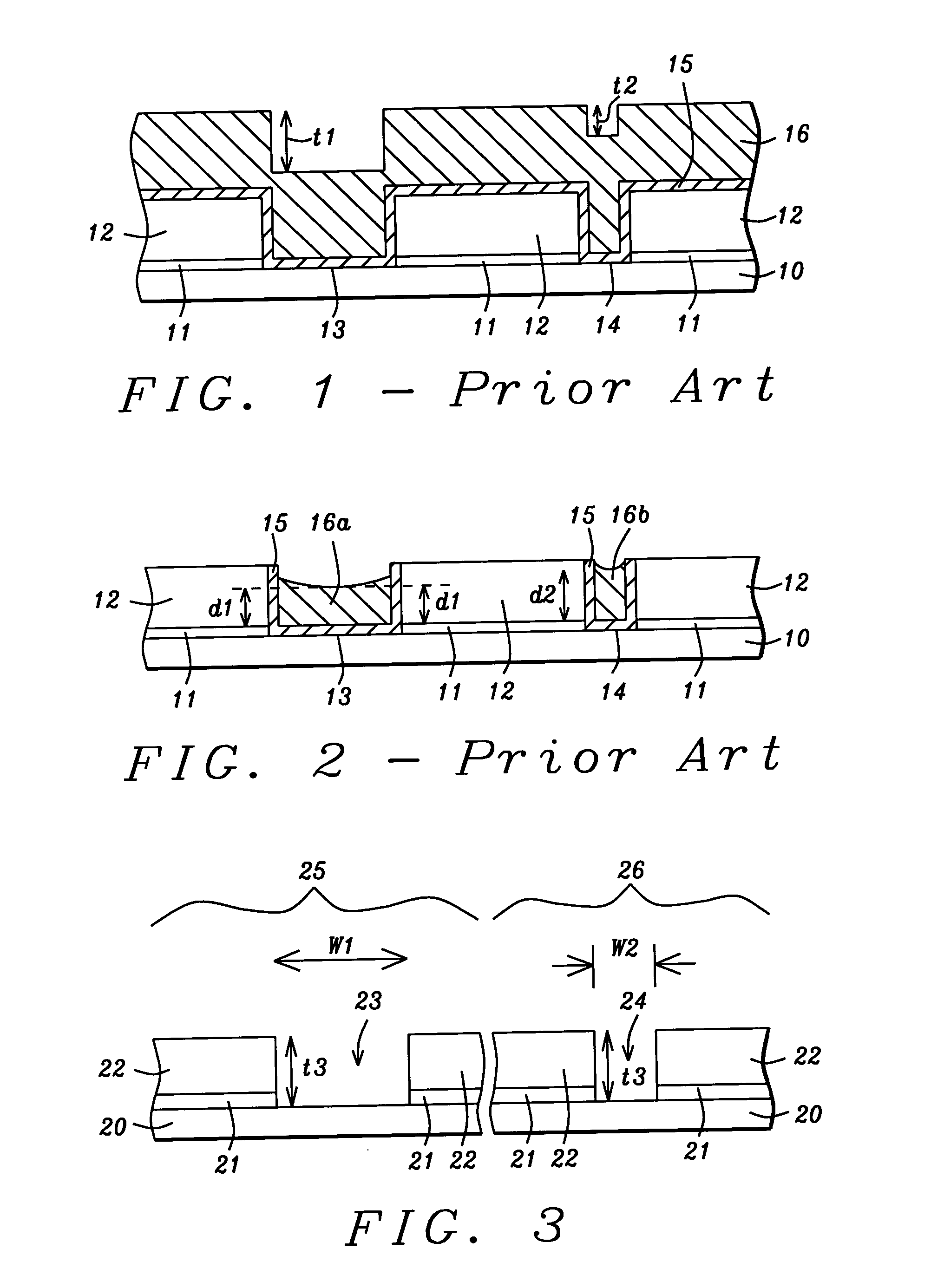
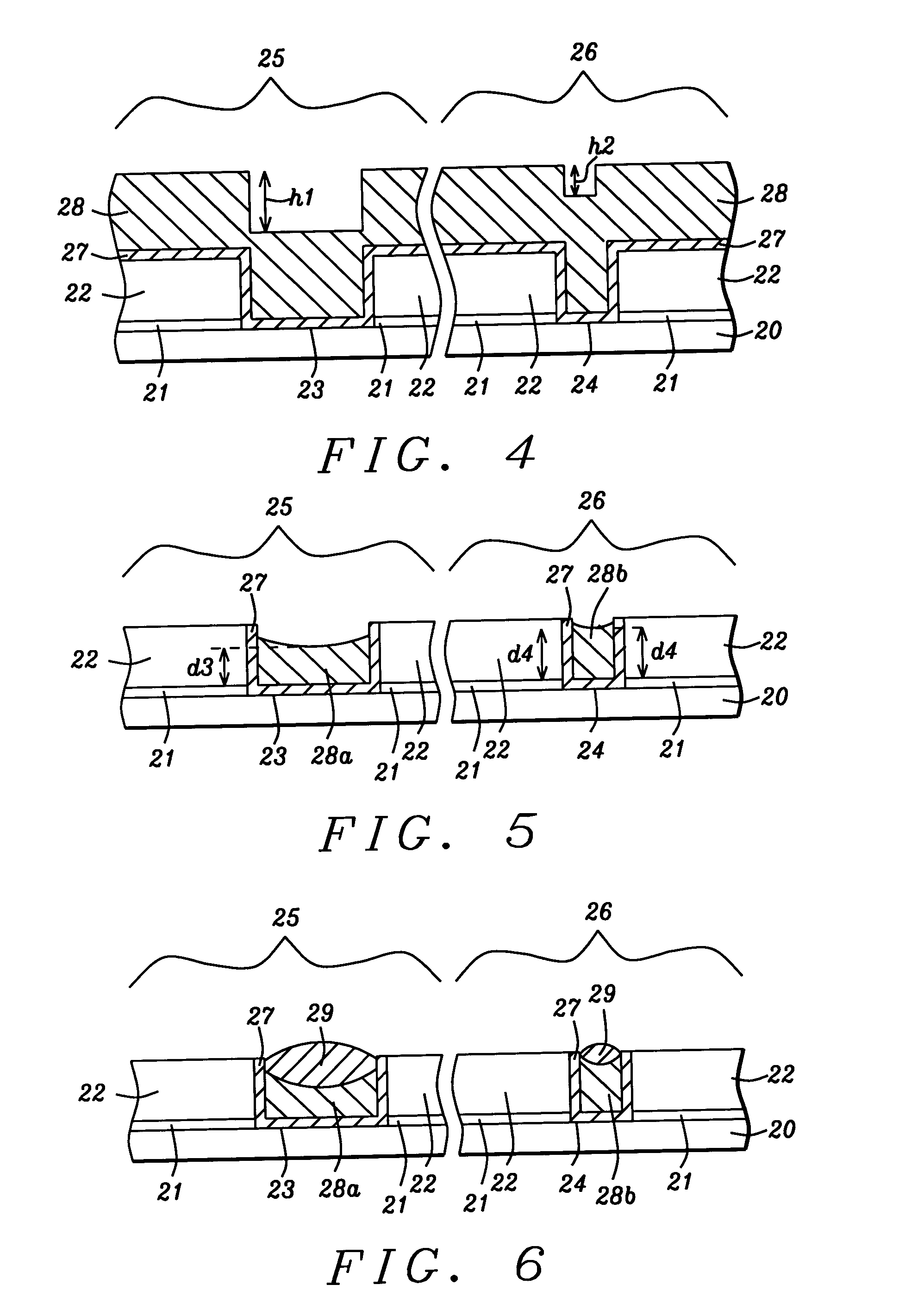
[0019] A first copper layer in a region of high pattern density is thinner than a first copper layer in a region with low pattern density. To solve this nonuniformity problem, a second copper layer is deposited on the first copper layer by a selective electroplating process which fills the openings and forms a dome shape above the openings. An anneal process is employed to ensure a good interface between the first and second copper layers and to promote a more uniform copper grain size in the second copper layer. A second CMP step which is an oxide buffing process is used to planarize the second copper layer which becomes coplanar with the adjacent dielectric layer. The combined thickness of the first and second copper layers is nearly independent of pattern density and copper linewidth and thereby affords a more uniform Rs across the substrate.

Problems solved by technology

A high polishing rate often leads to dishing or a dent in the copper surface so that the Cu level is below the surface of a surrounding dielectric layer.
Dishing is unacceptable because the cross-sectional area of a copper line is related to Rs and dishing causes Rs variations that detract from device performance.
There is currently no useful method in manufacturing to correct the non-planarity of the copper layers 16a, 16b.
As a result, the copper layer 16a has an unacceptably high Rs value and the Rs for the copper layer 16a is significantly larger than the Rs for the copepr layer 16b which will lead to device reliability and performance issues.
However, the first CMP step that is used to remove the seed layer on the surface of the substrate can be difficult to control since the underlying diffusion barrier layer is frequently too thin to function as a good CMP stop.
However, the method does not address a Rs nonuniformity problem associated with different metal pattern densities or different metal widths in the same layer.
However, the method does not address the effect of different pattern densities or trench width variations on Rs.

Method used


Image

  • Novel method to reduce Rs pattern dependence effect
  • Novel method to reduce Rs pattern dependence effect
  • Novel method to reduce Rs pattern dependence effect

Examples


first embodiment

[0028] The present invention is a method that is particularly useful in forming copper interconnects with improved Rs uniformity and thickness. Although the drawings relating to the first embodiment depict a single damascene scheme, the present invention is also applicable to a dual damascene fabrication sequence. Moreover, the method of the present invention may be repeated a plurality of times on the same substrate to form a succession of copper interconnect layers that are arranged in a stacked design as is appreciated by those skilled in the art. The drawings are provided as examples only and are not intended to limit the scope of the invention.

[0029] A first embodiment is depicted in FIGS. 3-7. Referring to FIG. 3, a substrate 20 is provided that typically includes active and passive devices as well as conductive and dielectric layers that are not shown in order to simplify the drawing. Substrate 20 is preferably silicon but may also be based on silicon-germanium, gallium-arsen...

second embodiment

[0043] the present invention is depicted in FIGS. 8-12 in which high and low copper density regions are formed on the same substrate and are comprised of copper interconnects that have equivalent width. The collective surface area of interconnects formed in a high density region is greater than about 35% of the area of the region. The collective surface area of interconnects formed in a low density region is less than about 30% of the area of the region.

[0044] Referring to FIG. 8, a substrate 30 is provided that typically includes active and passive devices as well as conductive and dielectric layers that are not shown in order to simplify the drawing. Substrate 30 is preferably silicon but may also be based on silicon-germanium, gallium-arsenide, or silicon-on-insulator technology. An etch stop layer 31 with a thickness from about 100 to 2000 Angstroms is deposited on substrate 30 by a CVD or PECVD method and is comprised of silicon nitride, silicon oxynitride, or silicon carbide. ...


PUM


Abstract

A method of forming a copper interconnect in an opening within a pattern is described. The copper interconnect has an Rs that is nearly independent of opening width and pattern density. A first copper layer having a concave upper surface and thickness t1 is formed in a via or trench in a dielectric layer by depositing copper and performing a first CMP step. A second copper layer with a thickness t2 where t2≦t1 and having a convex lower surface is deposited on the first copper layer by a selective electroplating method. The first and second copper layers are annealed and then a second CMP step planarizes the second copper layer to become coplanar with the dielectric layer. The invention is also a copper interconnect comprised of the aforementioned copper layers where the first copper layer has a grain density (GD1)≧GD2 for the second copper layer.

Description

FIELD OF THE INVENTION [0001] The invention relates to a method of fabricating copper interconnects with improved performance and in particular to a method of forming a plurality of interconnects having different widths and varying pattern densities but with a similar thickness so that sheet resistance (Rs) variation is minimized. BACKGROUND OF THE INVENTION [0002] Integrated circuits in a semiconductor device are comprised of metal wiring that is insulated by one or more dielectric layers to prevent capacitance coupling or crosstalk between the electrical pathways. Metal wiring that forms interlevel and intralevel connections which are commonly referred to as interconnects is frequently formed by depositing a metal in an opening such as a via hole or a trench in a single damascene approach or in a trench and via simultaneously in a dual damascene scheme. Usually, a diffusion barrier layer is formed on the sidewalls of the dielectric layer adjacent to the via and / or trench before me...

Claims


Application Information

Patent Timeline
IPC IPC(8): H01L21/22H01L21/288H01L21/38H01L21/44H01L21/4763H01L21/768
CPCH01L21/288H01L21/76877H01L21/7684
Inventor TSAO, JUNG-CHIHLI, CHI-WENCHEN, KEI-WEIHSU, JYE-WEIFONG, HSIEN-PINLIN, STEVENCHUANG, RAY
Owner TAIWAN SEMICON MFG CO LTD
Learn More