Method for measuring nm-scale tip-sample capacitance

a capacitance and nm-scale technology, applied in the direction of resistance/reactance/impedence, instruments, scanning probe techniques, etc., can solve the problem that existing scm circuits are typically not adapted for calibrated low frequency absolute capacitance measurements, and achieve accurate measurement of af-level variations and stray capacitance artifacts.

Inactive Publication Date: 2005-04-14
THE OHIO STATES UNIV
View PDF8 Cites 6 Cited by
  • Summary
  • Abstract
  • Description
  • Claims
  • Application Information

AI Technical Summary

Benefits of technology

Practically any drive frequency may be used when practicing this invention. In one embodiment, the power supply may be adapted to provide a low frequency AC voltage. For instance, the power supply may be adapted to provide a sinusoidal voltage having a frequency of between about 3 kHz and about 7 kHz. However, it should be recognized that the drive frequency may be less than 3 kHz or greater than 7 kHz. For instance, the drive frequency may be about 1 MHz. Certain embodiments of the present invention may perform better at higher drive frequencies. In particular, a higher drive frequency may result in a larger displacement current which is easier to measure.
The probe-sample current may include a displacement current that flows through a capacitance Cstray between the sample and the probe. In such an embodiment, the step of adding the probe-sample current and the bucking current may result in the bucking current substantially negating the displacement current that flows through the capacitance Cstray. A purpose of negating the displacement current that flows through Cstray is to allow the current amplifier to be operated at a high gain / low noise setting without overloading.
An exemplary embodiment of the instrumentation may be used to identify and characterize significant (e.g., greater than about 10 aF) variations in Cstray to facilitate accurate measurement of aF-level variations in the nm-scale tip-sample capacitance. In fact, the inventors have surprisingly discovered that Cstray varies with lateral probe position. This is due to tilting of the probe assembly as the piezo-electric scanner tube bends during scanning. The inventors have also surprisingly found that Cstray varies significantly with probe-assembly height. This causes topography related artifacts in capacitance images of rough surfaces. Nevertheless, in certain embodiments of the present invention, stray capacitance artifacts can be mostly eliminated by properly characterizing position and height dependent variations in Cstray and subtracting them from measured capacitance data.

Problems solved by technology

In other words, existing SCM circuits are typically not adapted for calibrated low frequency measurements of absolute capacitance.
However, not all systems of interest contain a semiconductor space-charge layer that exhibits voltage dependent capacitance.

Method used


Image

  • Method for measuring nm-scale tip-sample capacitance
  • Method for measuring nm-scale tip-sample capacitance
  • Method for measuring nm-scale tip-sample capacitance

Examples


Embodiment Construction

)

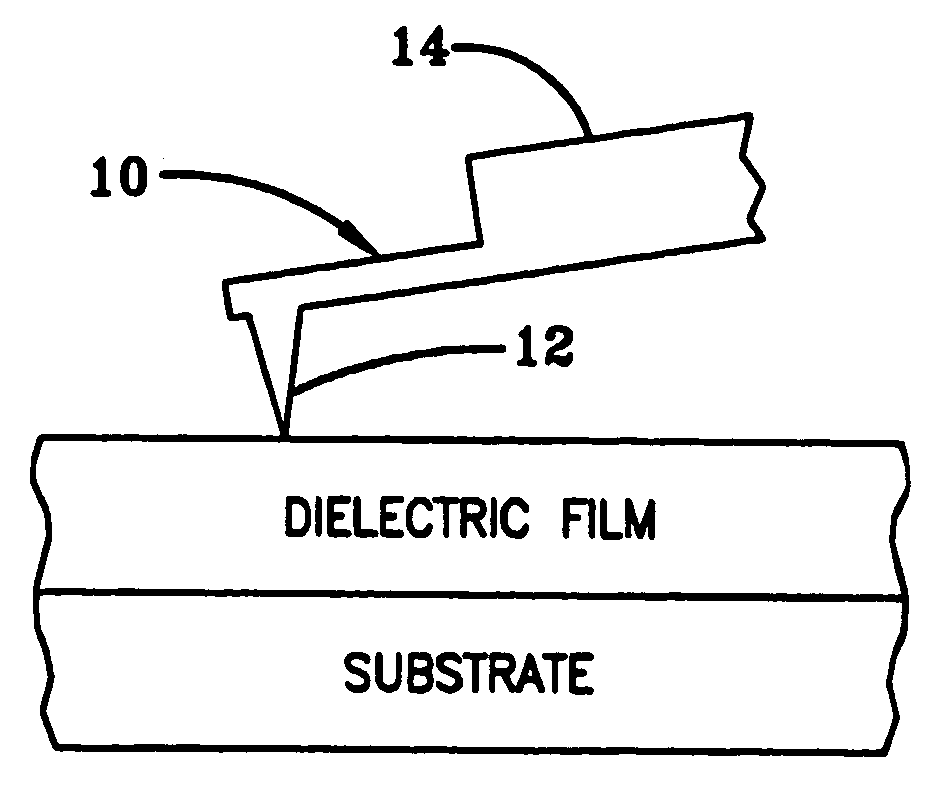
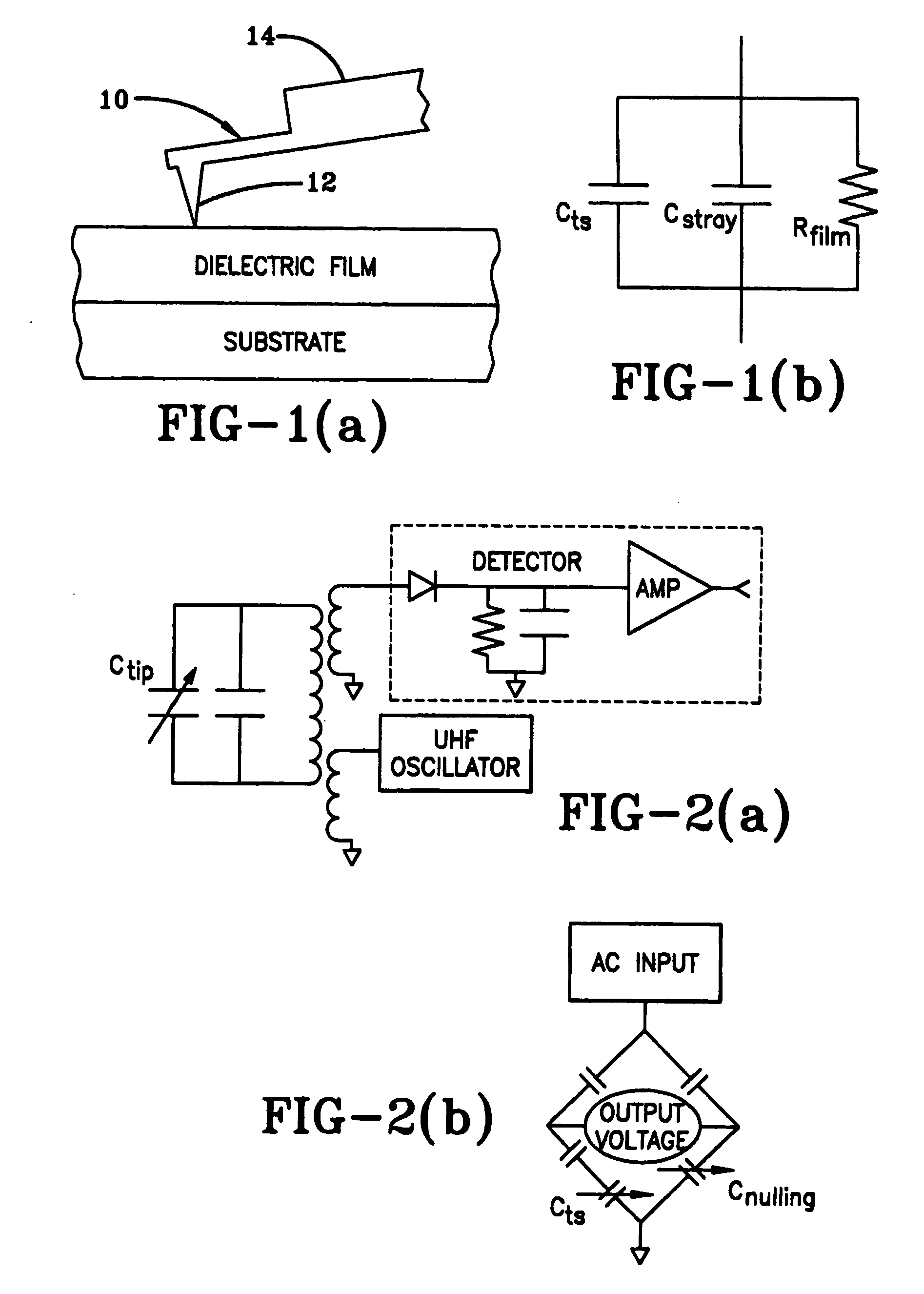
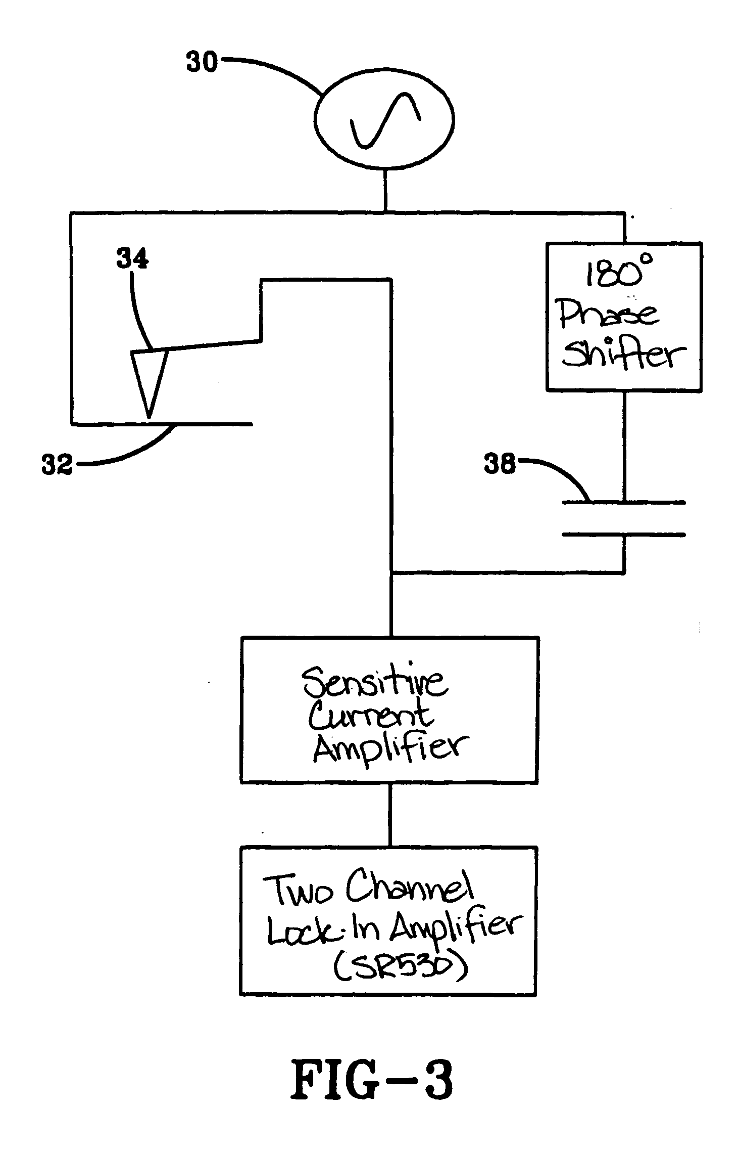
The present invention is directed to a system and method for measuring capacitance. The present invention may be useful for SCM and any other field in which it is desired to measure capacitance. In one exemplary embodiment of the present invention, a system comprised of commercially available electronics is provided that can measure the capacitance with sub-aF / {square root}{square root over (Hz)} noise levels at frequencies down to 1 Hz. However, it should be recognized that the system may be adjusted to measure capacitance with practically any desired noise levels at practically any desired frequencies. An exemplary embodiment of the present invention can also distinguish between displacement and leakage current. Furthermore, an exemplary embodiment of the present invention can characterize the noise in the system.

The present invention may also take into account how the long-range stray capacitance between the sample and the mm-sized probe assembly varies with the lateral and v...


PUM


Abstract

A method for measuring nm-scale tip-sample capacitance comprising: (a) measuring a cantilever deflection and a change in probe-sample capacitance relative to a reference level as a function of a probe assembly height; (b) fitting out-of-contact data to a function; (c) subtracting the function from capacitance data to get a residual capacitance as a function of the probe assembly height; and (d) determining the residual capacitance at a z-position where the cantilever deflection is zero.

Description

BACKGROUND OF THE INVENTION The present invention relates generally to a system and method for measuring capacitance. More particularly, the present invention relates to a system and method for measuring capacitance between a probe and a semiconductor sample. The present invention may be useful in the field of scanning capacitance microscopy (SCM). In a typical embodiment of SCM, a nanometer scale-conducting tip is scanned across a sample surface, and a capacitance detector measures variations in the probe-sample capacitance C. To date, some of the most common applications of SCM have been semiconductor characterization including dopant profiling, device characterization, and surface defect characterization. A common thread in these measurements is that the samples exhibit voltage dependent capacitance due to a voltage-dependent space charge layer in the semiconductor substrate. These implementations of SCM generally do not measure C directly. Rather, they typically measure dC / dV ...

Claims


Application Information

Patent Timeline
Patent Type & Authority Applications(United States)
IPC IPC(8): G01R27/26G01Q60/00
CPCB82Y35/00Y10S977/866G01R27/2605G01Q60/46
Inventor PELZ, JONATHAN P.LEE, DAVID T.BHUSHAN, BHARAT
Owner THE OHIO STATES UNIV
Why Eureka
Try Eureka