Electrostatic discharge protection for integrated circuit devices

Inactive Publication Date: 2005-03-03
AGENCY FOR SCI TECH & RES
View PDF5 Cites 36 Cited by
  • Summary
  • Abstract
  • Description
  • Claims
  • Application Information

AI Technical Summary

Benefits of technology

[0009] In accordance with a first aspect of the present invention, there is provided an apparatus for providing ESD protection to an integrated circuit d vice. The apparatus comprises a substrate made of a first type of semiconductor, a first region of a complementary type of semiconductor formed in the substrate, and a plurality of second regions of said one type of semiconductor formed in the first region. In each of the plurality of second regions, there is formed a diode. The first region is disposed between the plurality of second regions and the substrate and therefore, the plurality of second regions do not directly contact the substrate so that signal leakage to the substrate is reduced. The plurality of diodes can be selectively connected in series for coupling to the integrated circuit device to provide ESD protection thereto.
[0013] Each one of the plurality of second regions and the first region form a parasitic diode, and each one of the plurality of second regions, the first region and the substrate form a bipolar device. The bipolar device is coupled between the parasitic diode and the substrate, so that a current leakage from the parasitic diode to the substrate is reduced.
[0014] In accordance with a second aspect of the present invention, there is provided an integrated circuit device with on-chip ESD-protection circuits. The device comprises a substrate, a functional module formed on the substrate and a plurality of diodes formed in a plurality of a second well structures of the substrate. A first well structure is disposed between the plurality of the second well structures and the substrate for preventing direct connection or contact between the second well structures and the substrate. Signal leakage between the diodes and the substrate is reduced, therefore the diodes are capable to be connected in series to form a diode string. The diode string has an increased overall turn-on voltage which is higher than the operational signal level of the functional module so that during normal operation, the diode string will not be turned on to leak normal signals.
[0017] The present invention advantageously utilizes well / deep well structure to prevent direct contact or connection between the P-N structure of diode and the substrate and overcome the problem of signal leakage due to the parasitic diodes in CMOS technology. Diodes are successfully connected in series in CMOS technology to provide ESD protection for devices with signal applications level higher than the turn-on voltage of a single diode.

Problems solved by technology

When used in an RFPA for ESD protection, this single diode may be turned-on, resulting in the leakage of the normal signal.
Therefore, signal loss and / or distortion can occur which will seriously affect the normal operations of the IC device.
Unfortunately, the attempt of directly connecting two or more diodes in series faces difficulties and problems in CMOS technology.
As such, connecting P+ / N-well diodes in series with is not suitable to provide ESD protection for relatively large signal electronic devices.

Method used


Image

  • Electrostatic discharge protection for integrated circuit devices
  • Electrostatic discharge protection for integrated circuit devices
  • Electrostatic discharge protection for integrated circuit devices

Examples


Embodiment Construction

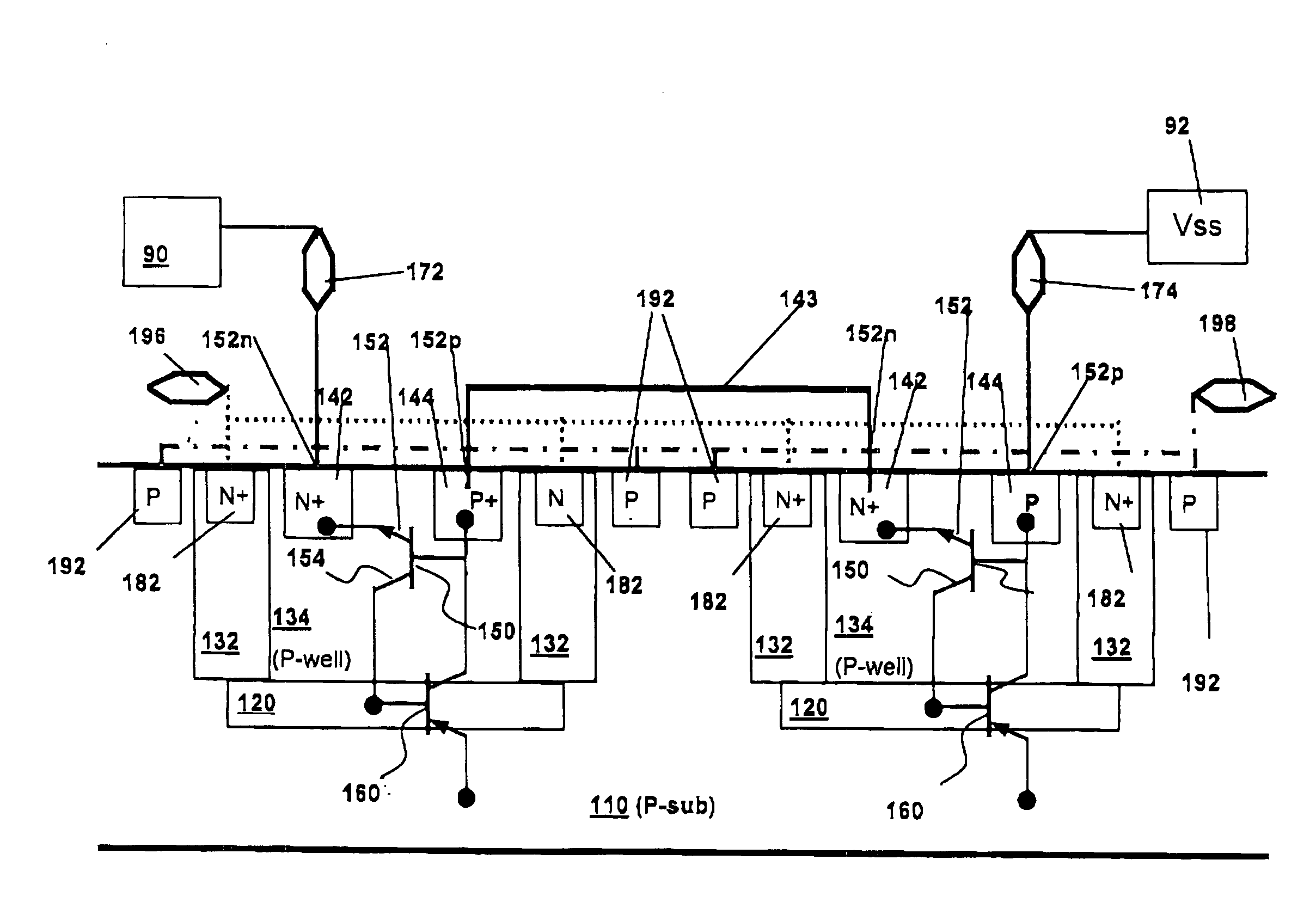
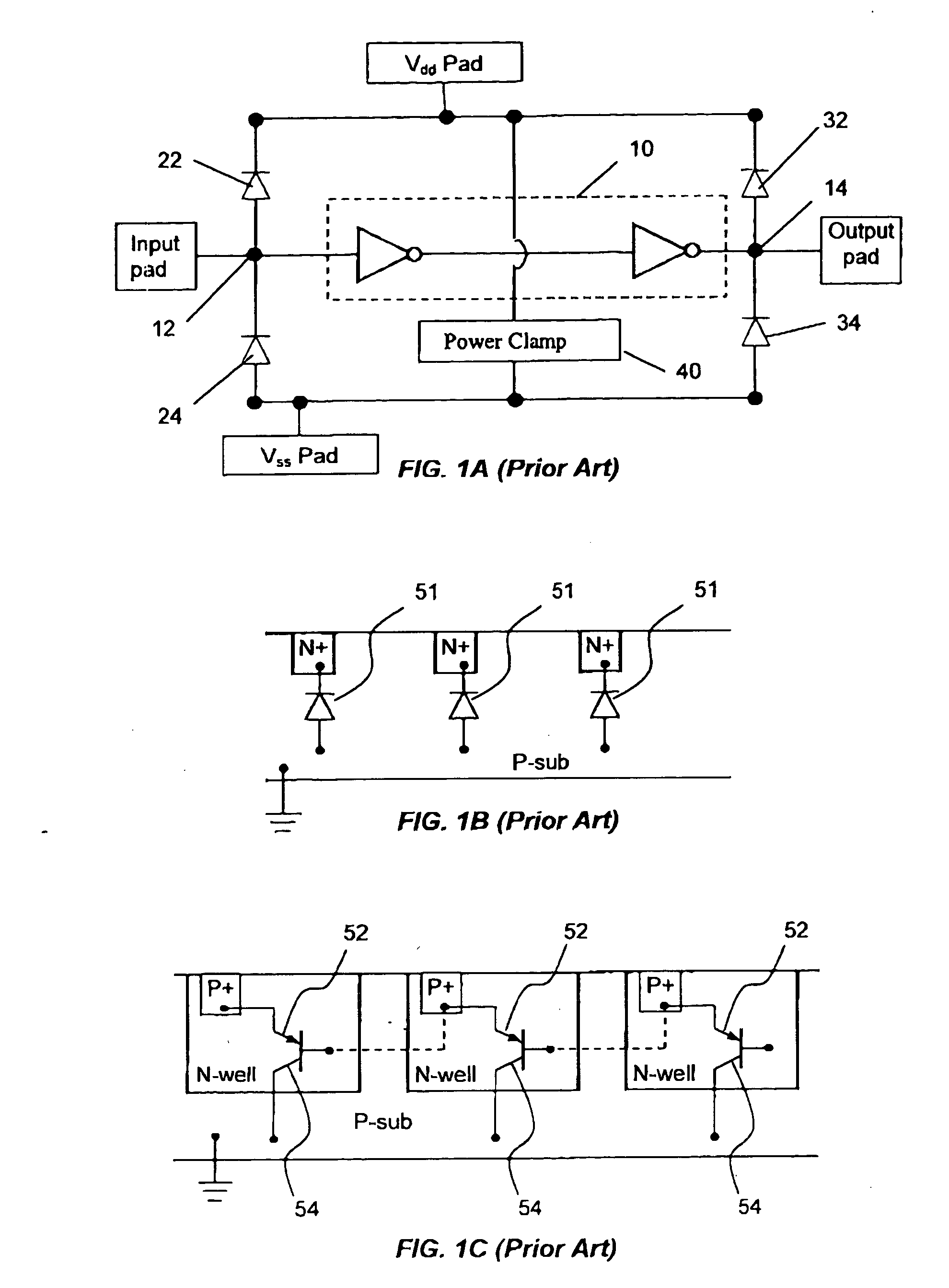
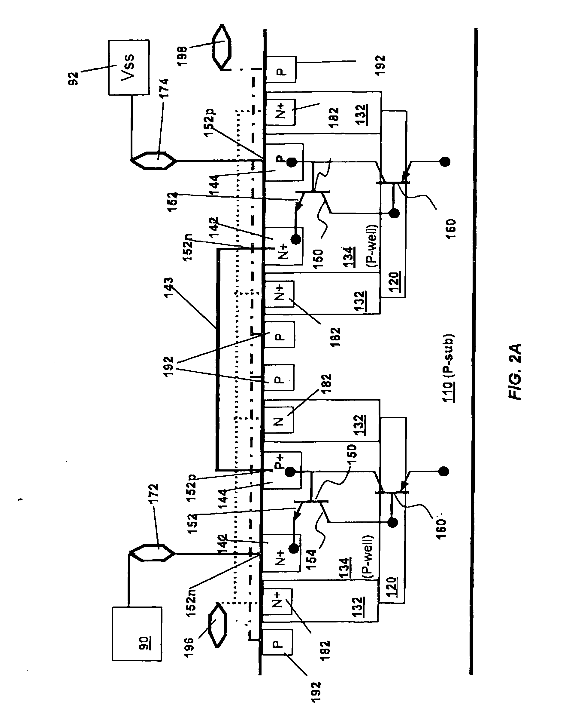
[0026] As shown in FIGS. 2A and 2B, an ESD protection apparatus 100 for a semiconductor device 90 (such as a CMOS device) according to one embodiment of the present invention comprises a semiconductor substrate 110, such as a P-type semiconductor. A plurality of deep N-wells 120 and N-wells 132 are formed on the substrate 110. A plurality of P-wells 134 are formed in each deep N-well 120 and N-wells 132. Although only two P-wells 134 are shown for ease of illustration, many additional P-wells may be formed, either in the same or separate deep N-wells / N-wells. One pair of N+ and P+ regions 142, 144 is formed in each one of the plurality of P-well 134.

[0027] N+ and P+ regions 142, 144 in each P-well 134 form diodes 152, each having an N-node 152n and a P-node 152p. Formed by P+ regions 144 / P-wells 134 and deep N-wells 120 / N-wells 132 are parasitic diodes 154. Each diode 152 and parasitic diode 154 form an NPN bipolar 150. Similarly, formed by P+ regions 144 / P-wells 134, deep N-wells ...


PUM


Abstract

An apparatus for providing ESD protection to an integrated circuit device comprising a substrate of one type of semiconductor, a first region of a complementary type of semiconductor formed in the substrate, which surrounds a second region of said one type of semiconductor. A plurality of diodes each is formed in one of the plurality of second regions. The at least one first region is disposed between the plurality of second regions and the substrate to prevent direct contact between the second regions and the substrate. The plurality of diodes are connectable in series for coupling to the integrated circuit device for providing ESD protection.

Description

FIELD OF THE INVENTION [0001] The present invention relates to electrostatic discharge protection for electronic devices. In particular, it relates to electrostatic discharge protection structure for integrated circuit devices such as complementary metal oxide semiconductor (CMOS) devices. BACKGROUND OF THE INVENTION [0002] Electrostatic discharge (ESD) commonly occurs during the manufacturing, handling and using of electronics devices, such as integrated circuit (IC) devices or chips. ESD may cause an electrical pulse that exceeds the withstanding limit of an IC chip and cause failure or damage of the device Effective ESD protection at each and every pin-out of an IC chip therefore becomes a key concern during the designing and manufacturing of IC chips. [0003] A number of conventional methods are available for providing IC devices with ESD protection, some of which utilize diodes. FIG. 1A is a schematic diagram showing a general ESD protection scheme for an IC device 10 using diod...

Claims


Application Information

Patent Timeline
IPC IPC(8): H01L27/02H01L29/74
CPCH01L29/87H01L27/0262
Inventor ZHANG, WEIMIN
Owner AGENCY FOR SCI TECH & RES
Why Eureka
Try Eureka