Low k interconnect dielectric using surface transformation

Inactive Publication Date: 2005-02-10
MICRON TECH INC
View PDF68 Cites 16 Cited by
  • Summary
  • Abstract
  • Description
  • Claims
  • Application Information

AI Technical Summary

Benefits of technology

The above mentioned problems are addressed by the present subject matter and will be understood by reading and studying the following specification. The present subject matter provides a low-k dielectric insulator for integrated circuit interconnects that is easily prepared, that is consistently formed and that does not suffer from high internal stress and cracking. The low-k dielectric insulator of the present invention includes empty spaces formed using surface transformation. As such, the present invention provides a system and method that improves integrated circuit performance by reducing the interconnect RC time constant.

Problems solved by technology

One particular problem confronting the semiconductor industry is that, as integrated circuit scaling continues, the performance improvement is limited by the signal delay time attributable to interconnects in the integrated circuit.
However, even though the delay attributable to the gates continues to decrease as scaling continues beyond the 0.18 μm technology, the overall delay increases significantly because the interconnect delay is significantly increased.
However, it is difficult to control the preparation of Xerogel and Aerogel low-k films.
Furthermore, large amounts of liquid solvents and non-solvents have to be removed to form the voids, which tend to produce variability in the void size, shape and density, and tend to produce shrinkage that can cause high internal stress and cracking.

Method used


Image

  • Low k interconnect dielectric using surface transformation
  • Low k interconnect dielectric using surface transformation
  • Low k interconnect dielectric using surface transformation

Examples


Embodiment Construction

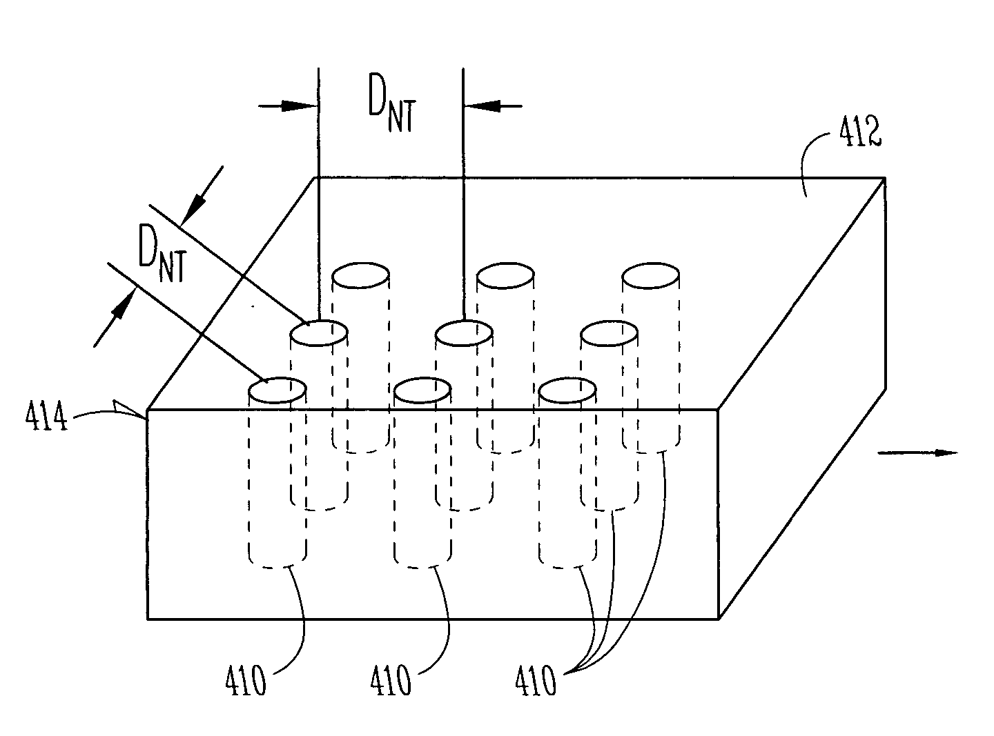
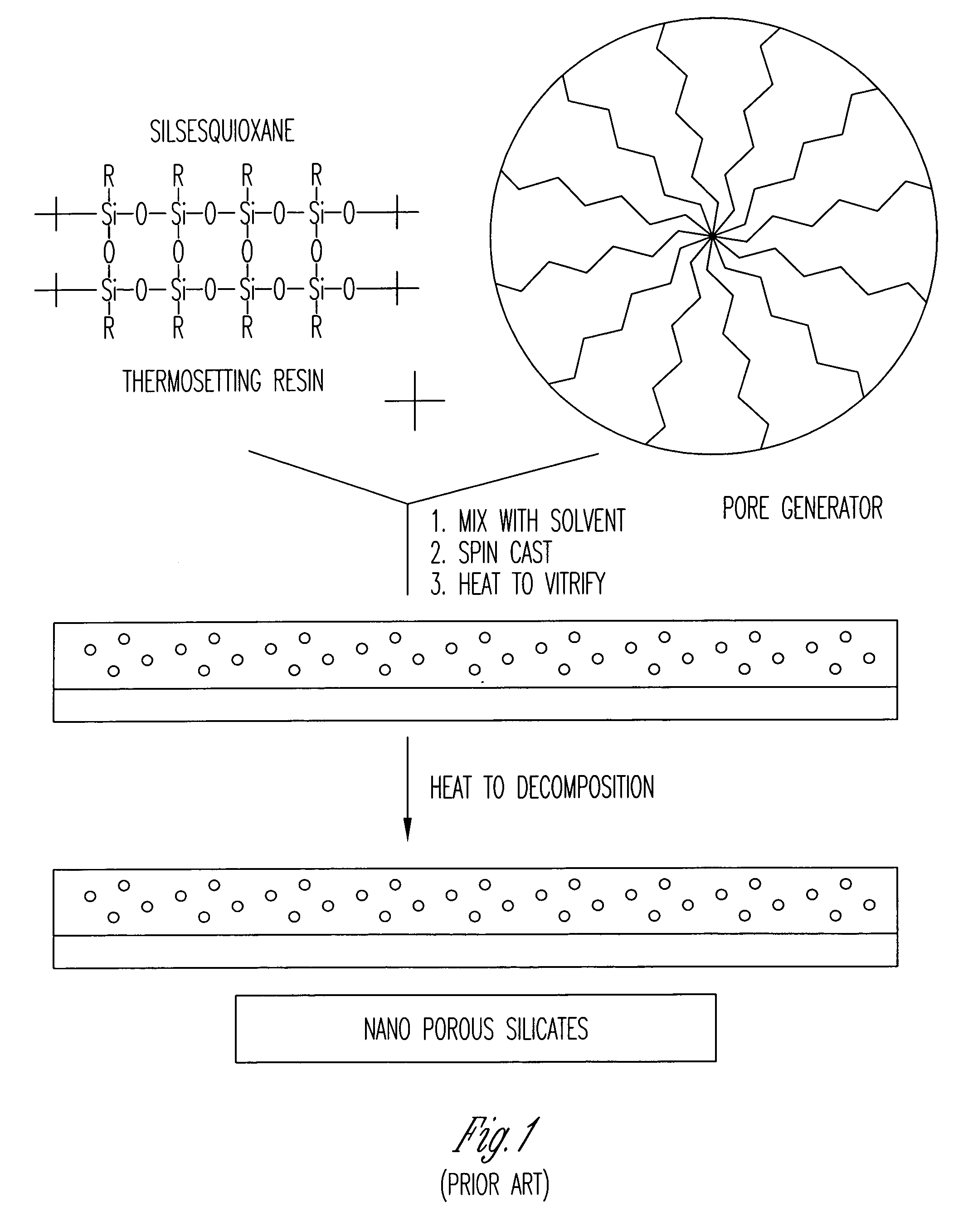
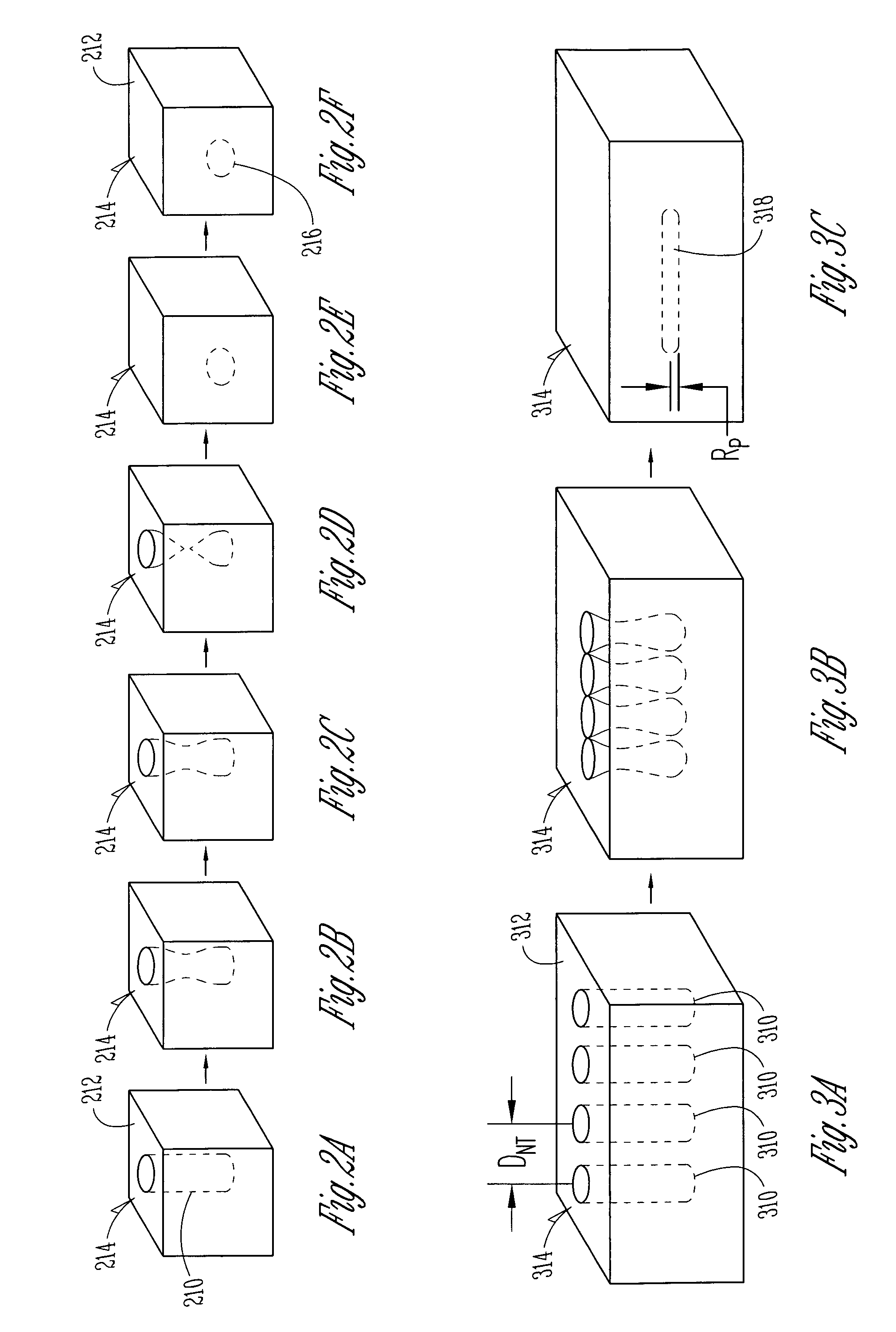
The following detailed description of the invention refers to the accompanying drawings which show, by way of illustration, specific aspects and embodiments in which the invention may be practiced. In the drawings, like numerals describe substantially similar components throughout the several views. These embodiments are described in sufficient detail to enable those skilled in the art to practice the invention. Other embodiments may be utilized and structural, logical, and electrical changes may be made without departing from the scope of the present invention. The following detailed description is, therefore, not to be taken in a limiting sense, and the scope of the present invention is defined only by the appended claims, along with the full scope of equivalents to which such claims are entitled.

The present subject matter improves integrated circuit performance by reducing the RC time delays attributable to interconnects. The present subject matter provides a low-k dielectric ...


PUM


Abstract

Systems, devices and methods are provided to improve performance of integrated circuits by providing a low-k insulator. One aspect is an integrated circuit insulator structure. One embodiment includes a solid structure of an insulator material, and a precisely determined arrangement of at least one void formed within the solid structure which lowers an effective dielectric constant of the insulator structure. One aspect is a method of forming a low-k insulator structure. In one embodiment, an insulator material is deposited, and a predetermined arrangement of at least one hole is formed in a surface of the insulator material. The insulator material is annealed such that the low-k dielectric material undergoes a surface transformation to transform the arrangement of at least one hole into predetermined arrangement of at least one empty space below the surface of the insulator material. Other aspects are provided herein.

Description

TECHNICAL FIELD OF THE INVENTION This invention relates generally to integrated circuits and, more particularly, to integrated circuit dielectrics useful for reducing the signal delay time attributable to interconnects. BACKGROUND OF THE INVENTION The semiconductor industry continuously strives to reduce the size and cost of integrated circuits. One method for measuring the performance of an integrated circuit uses the maximum clock speed at which the circuit operates reliably, which depends on how fast transistors can be switched and how fast signals can propagate. One particular problem confronting the semiconductor industry is that, as integrated circuit scaling continues, the performance improvement is limited by the signal delay time attributable to interconnects in the integrated circuit. According to one definition, integrated circuit interconnects are three-dimensional metal lines with submicrometer cross sections surrounded by insulating material. One definition of an in...

Claims


Application Information

Patent Timeline
IPC IPC(8): H01L21/3105H01L21/311H01L21/312H01L21/316H01L21/768H01L23/532
CPCH01L21/0212H01L21/02145H01L2924/0002H01L21/02161H01L21/02203H01L21/02266H01L21/02354H01L21/31058H01L21/31138H01L21/3122H01L21/31695H01L21/7682H01L23/5329H01L2924/00H01L21/02126H01L21/02282
Inventor GEUSIC, JOSEPH E.FARRAR, PAUL A.BHATTACHARYYA, ARUP
Owner MICRON TECH INC
Why Eureka
Try Eureka