Eureka AIR delivers breakthrough ideas for toughest innovation challenges, trusted by R&D personnel around the world.

Nonvolatile memory device with sense amplifier securing reading margin

a sense amplifier and non-volatile memory technology, applied in static storage, digital storage, instruments, etc., can solve the problems of deformation of elements, broken thin insulating film forming tmr elements, and inability to perform data reading

Inactive Publication Date: 2004-05-20
RENESAS ELECTRONICS CORP
View PDF9 Cites 34 Cited by
  • Summary
  • Abstract
  • Description
  • Claims
  • Application Information

AI Technical Summary

Benefits of technology

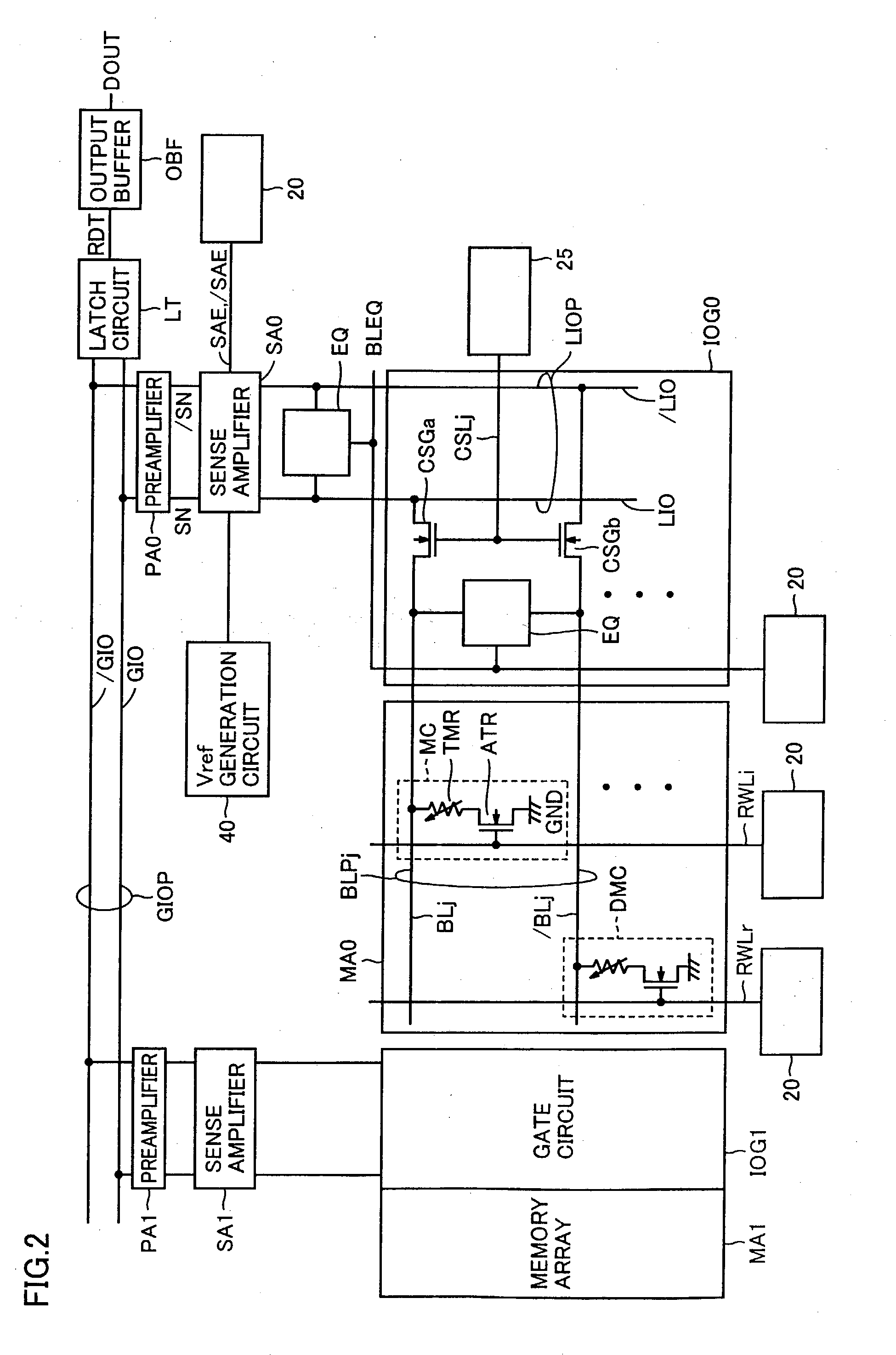
[0012] According to the present invention, as described above, the differential amplifying unit adjusts the voltages of the first and second data lines by the first and second current mirror circuits. The first and second current mirror circuits supply mirror currents according to the passing currents which flow through the first and second data lines to the first and second internal nodes, and the amplifying unit outputs read data according to the mirror current difference. With the configuration, adjusting the voltage to be applied to the selected memory cell which is connected to one of the first and second data lines makes it possible to perform stable data reading and also perform a data read operation based on a small amount of passing current. It is therefore possible to operate at a low voltage and to reduce power consumption of the differential amplifying unit.
[0014] According to the present invention, X data lines are provided and a plurality of bit lines are divided into groups each consisting of X bit lines. Further, X connection control circuits are provided for electrically coupling the X bit lines in each group to the X data lines at the time of data reading, and the X connection control circuits are each provided with X differential amplification units which perform data reading in accordance with the difference in passing current between each data line and the reference current at the time of data reading. It is therefore possible to realize X-bit data reading from the X bit lines in one data read operation, and to perform efficient data reading.

Problems solved by technology

The data reading requires securing reading margin by increasing the amount of passing current; however, applying too much voltage may make it impossible to perform data reading.
For example, when a high voltage is applied to a tunneling magneto-resistance element (hereinafter, also referred to as a TMR element) which is a storage element of an MRAM device, there arises a problem in that the thin insulating film forming the TMR element is broken.
When a high voltage is applied to a chalcogenide layer used as a storage element of an OUM(R) device, there arises a problem in that the element is deformed, whereby the stored data is broken.
In addition, in a flash memory which performs data storage according to the level of a threshold voltage, when the amount of passing current which flows through the flash memory is increased too much by applying a high voltage, there arises a problem in that erroneous writing is caused, whereby stored data is broken.
Therefore, it is difficult to secure data reading margin with a low operating voltage.

Method used


Image

  • Nonvolatile memory device with sense amplifier securing reading margin
  • Nonvolatile memory device with sense amplifier securing reading margin
  • Nonvolatile memory device with sense amplifier securing reading margin

Examples


first embodiment

MODIFICATION OF FIRST EMBODIMENT

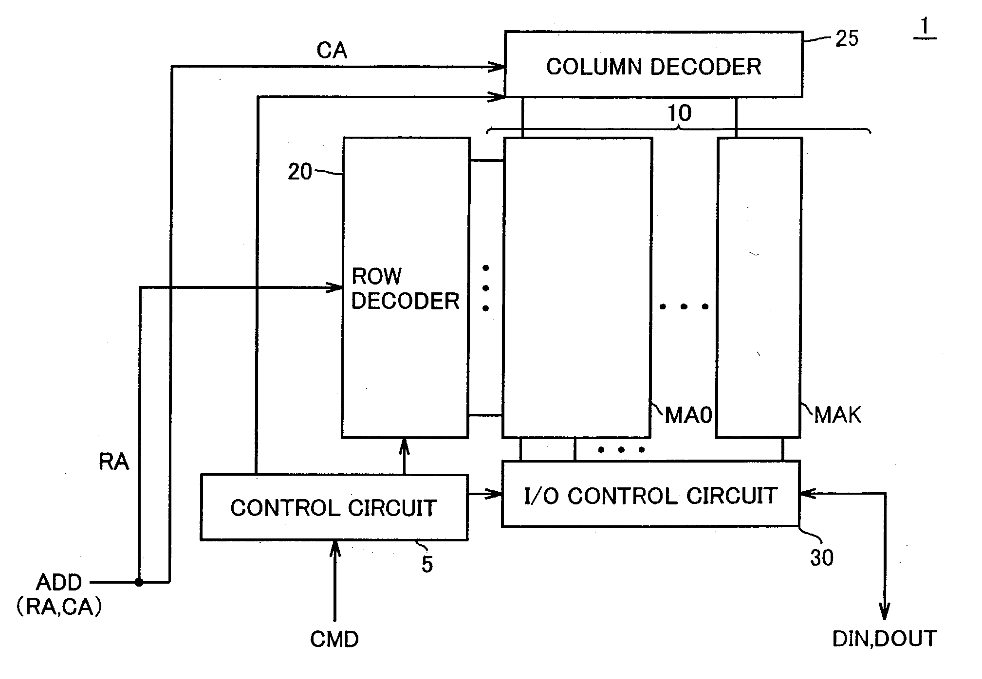
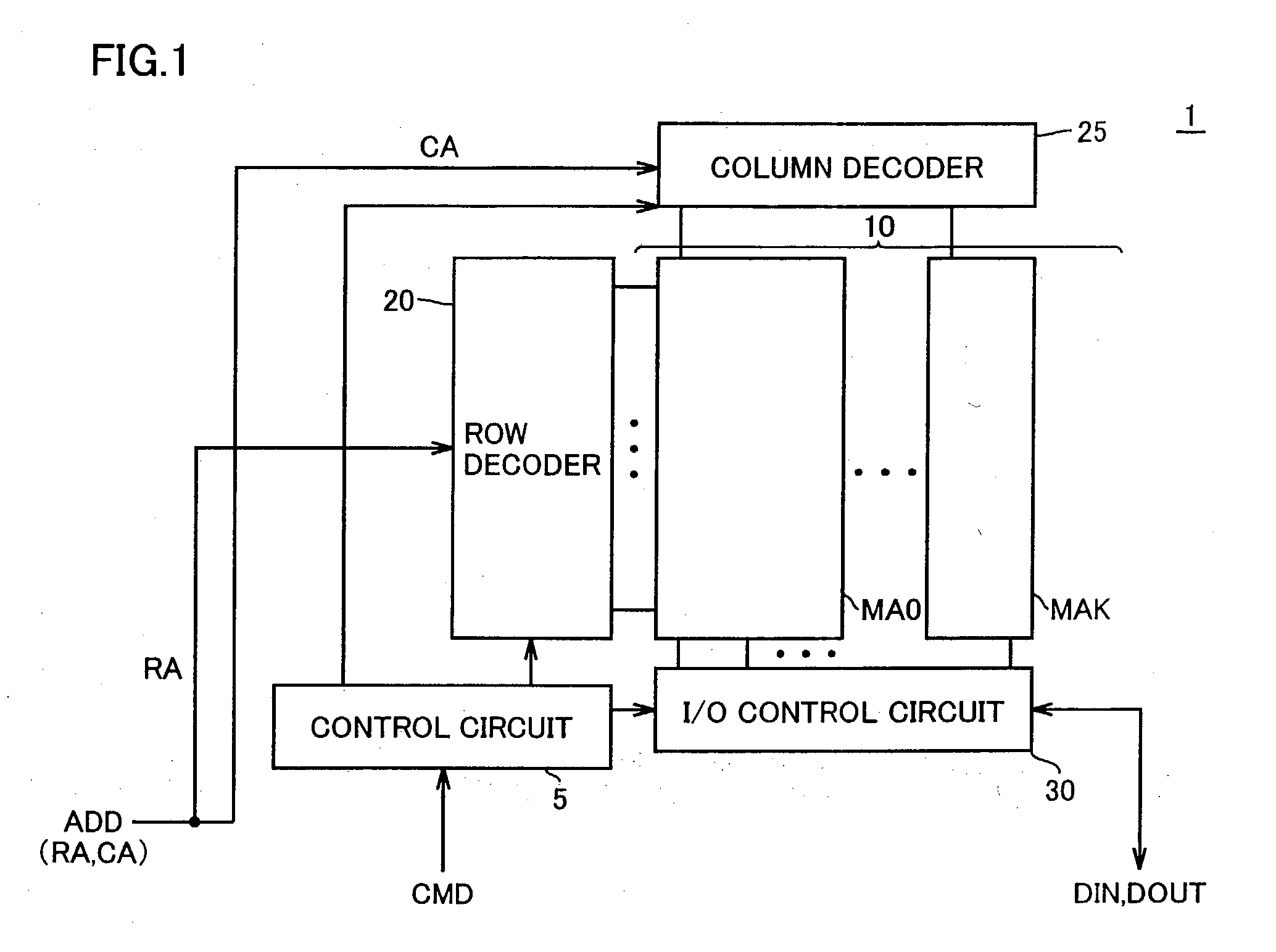
[0108] According to a modification of the first embodiment of the present invention, a description will be given of the configuration of data reading circuits in the case where memory cell MC is fixedly connected through access transistor ATR not to ground voltage GND but to power supply voltage Vcc.

[0109] With reference to FIG. 10, the data reading circuits according to the modification of the first embodiment of the present invention differ from the data reading circuits shown in FIG. 2 in that sense amplifiers SAQ uses in place of sense amplifiers SA. The other components, which have the same configuration, will not be repeatedly described. The present embodiment shows a sense amplifier SAQ0 provided in correspondence with memory array MA0 and a sense amplifier SAQ1 provided in correspondence with memory array MA1.

[0110] With reference to FIG. 11, the circuit configuration of sense amplifiers SAQ according to the modification of the first embodimen...

second embodiment

MODIFICATION OF SECOND EMBODIMENT

[0126] In the second embodiment, the description has been given of the configuration to reduce the power consumption of the sense amplifiers by activating control signal / SAE earlier than control signal SAE.

[0127] In a modification according to the second embodiment of the present invention, a description will be given of a configuration where control signal SAE is activated earlier than control signal / SAE.

[0128] With reference to the timing chart of FIG. 13, operations of the sense amplifier SA0 of the modified example according to the modification of the second embodiment of the present invention will be described.

[0129] Not being illustrated, after effective address ADD is inputted at time t1 in the same manner as in FIG. 9 according to the first embodiment, control signal SAE is set at "H" level at time t2. This causes sense nodes SN, / SN to start to make a transition to an intermediate potential between power supply voltage Vcc and ground volta...

third embodiment

[0133] In the first embodiment, the description has been given of the configuration of the data reading circuits for performing 1-bit data reading with sense amplifier SA0 corresponding to selected memory array MA0.

[0134] In a third embodiment, a description will be given of a configuration of the data reading circuits capable of performing parallel reading of plural-bit data.

[0135] With reference to FIG. 14, the data reading circuits according to the third embodiment of the present invention include a memory array MA#0 in place of memory array MA0.

[0136] A group of circuits for a data read operation are provided in correspondence with memory array MA#0 included in the I / O control circuit according to the third embodiment of the present invention. Memory array MA#0 will be taken up as an example and described. The other memory arrays, which have the same configuration, and therefore the description will not be repeated.

[0137] Memory array MA#0 has the plurality of memory cells MC an...


PUM


Abstract

In a sense amplifier, local I / O lines are maintained at a predetermined voltage by transistors. Transistors forming a current mirror supply an operating current according to a passing current which flows through transistors, to sense nodes. Transistors forming a current mirror extract an operating current according to the passing current which flows through transistors, from sense nodes. As a result, a voltage difference is generated in sense nodes in accordance with the operating current difference.

Description

[0001] 1. Field of the Invention[0002] The present invention relates to a nonvolatile memory device, and more particularly to a circuit configuration of a sense amplifier which amplifies storage data in a memory cell.[0003] 2. Description of the Background Art[0004] In recent years, a nonvolatile memory device enabling nonvolatile data storage is becoming mainstream. An example thereof includes a flash memory enabling high integration. Further, special attention is being given, as nonvolatile memory devices for the new generation, to an MRAM (Magnetic Random Access Memory) device for performing nonvolatile data storage with a thin film magnetic element, and an OUM(R) (Ovonic Unified Memories) device for performing data storage with a thin film material called chalcogenide.[0005] Data stored in a memory cell used as a storage element of these nonvolatile memory devices is generally read by applying a predetermined voltage on the storage element and detecting a passing current at the ...

Claims


Application Information

Patent Timeline
Patent Type & Authority Applications(United States)
IPC IPC(8): G11C11/15G11C7/06G11C7/14G11C11/16G11C16/28
CPCG11C7/04G11C7/062G11C2207/063G11C11/16G11C16/28G11C7/14
Inventor TANIZAKI, HIROAKIHIDAKA, HIDETOOOISHI, TSUKASA
Owner RENESAS ELECTRONICS CORP
Why Eureka
Eureka Blog
Learn More