
Nonlinear gold nanocluster chemical vapor sensor

a chemical vapor sensor and nanocluster technology, applied in nanoinformatics, instruments, material impedance, etc., can solve the problems of sacrificing reliability, miniaturization affinity, and low cos

Inactive Publication Date: 2004-02-12
THE UNITED STATES OF AMERICA AS REPRESENTED BY THE SECRETARY OF THE NAVY
View PDF5 Cites 15 Cited by
  • Summary
  • Abstract
  • Description
  • Claims
  • Application Information

AI Technical Summary

Benefits of technology

[0022] It is another object of the invention to provide materials, methods and equipment suitable for the sensitive and reliable detection or quantitation of a preselected chemical species in a target environment.
[0023] It is yet another object of the invention to provide materials, methods and equipment as aforesaid which are well-suited for applications requiring compact size, low cost and low power consumption.
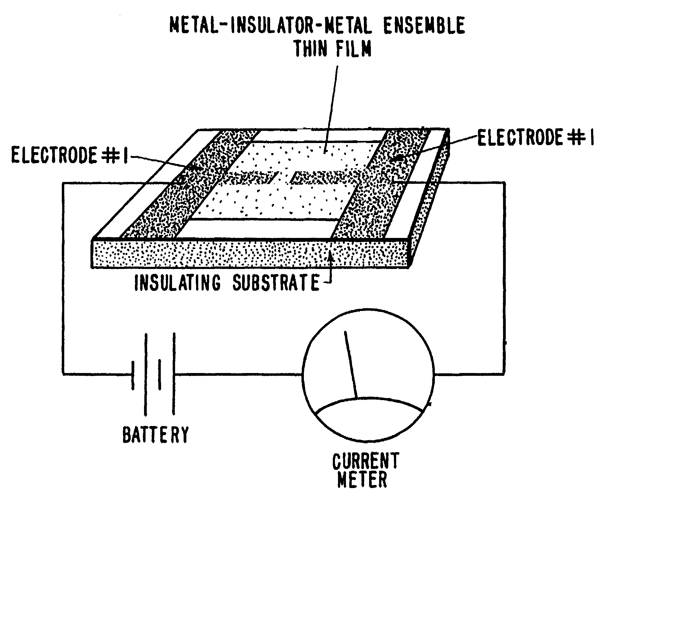
[0028] The electrodes are composed of metal deposited on the substrate. The top surface (at least) of the substrate must be insulating enough to ensure that essentially all of the current between the electrodes flows through the particle film and not through the substrate. The electrodes may be patterned in a variety of geometries but must be spaced no further than 0.1 .mu.m apart; the preferable spacings are in the range 10-50 nm. The electrodes can be defined using optical lithography by first defining widely-spaced electrodes and then doing a second, angled evaporation of metal that narrows the gap down to the size of the "shadow" cast by one of the original electrodes. Gaps in the range of 10-50 nm are easily achieved in this way. Even smaller gaps may be achieved using electroplating techniques. To make a device that not only has a small gap but also a narrow width, one can use standard electron beam lithography. In this case one creates "finger" electrodes with gaps down to 15 nm and widths as small as 25 nm. The reduced width limits the number of conduction paths and thereby strengthens the nonlinearity of the device.
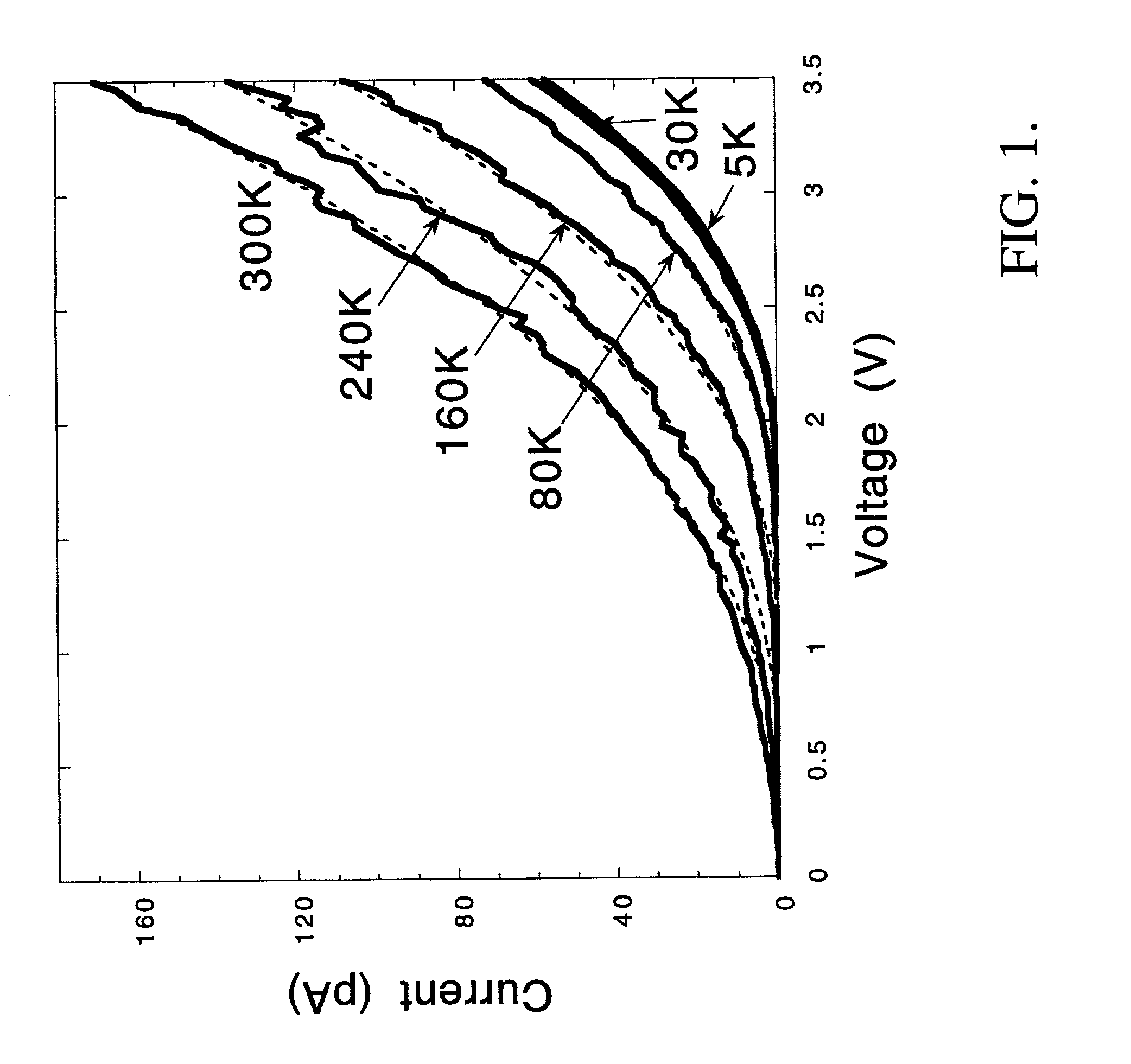
[0031] As noted earlier, the nonlinear chemiresistors of the present invention have much in common with micron-sized MIME sensors of U.S. Pat. No. 6,221,673. In particular, they take advantage of the fact that the particles that serve as the active elements of the micron-sized MIME sensors are extremely small. As a result, the micron-sized devices of the present invention are readily scaled to much smaller dimensions both laterally with more closely-spaced electrodes and vertically with much thinner cluster films including single-layer films. In addition, the small size of the metallic cores of the particles of the present invention means that they have large charging energies and hence can exhibit strong Coulomb blockade effects even at room temperature. Such effects are not observable in the micron-scaled devices because of the huge number of conduction paths that give rise to the overall signal. But as the device is scaled down to a relative few number of particles Coulomb blockade phenomena will come to dominate the behavior and this "new" physics regime can dramatically improve the sensitivity at a given power level of MIME-like chemical vapor sensors. Alternatively, it can achieve the same sensitivity but with much lower power dissipation.
[0032] Because the Coulomb-blockade-based chemical vapor sensor described herein passes near zero current when no vapor is present (yet gives a detectable signal upon vapor exposure), it will have ultra-low standby power. This also suggests that the sensor could operate as a digital device and hence require less signal conditioning when interfaced with a digital controller. When vapor is present the signal is strongly amplified by the nonlinear I-V characteristic of the device thus providing high sensitivity at ultra-low power levels. They could function for long periods of time utilizing very weak power sources when operating at pW levels. The sensor can also achieve high selectivity through proper chemical functionalization. Other advantages are: low cost (making possible extensive redundancy); rapid response times; ability to do submicron array sensing; and small thermal mass which provides an extra dimension for vapor detection and discrimination.

Problems solved by technology

However, it would still be desirable for the art to have an alternative detection technology which lends itself to ready and versatile implementation as well as consumes power at a very low level, without sacrificing reliability, miniaturization affinity, and low cost.

Method used


Image

  • Nonlinear gold nanocluster chemical vapor sensor
  • Nonlinear gold nanocluster chemical vapor sensor
  • Nonlinear gold nanocluster chemical vapor sensor

Examples


example

[0048] To demonstrate a Coulomb blockade-based nanocluster vapor sensor of the type depicted in FIG. 3, we carried out the fabrication as described above. In order to accentuate the charging effects responsible for Coulomb blockade-mediated detection, following self-assembly of the clusters onto the electronic substrate, an exchange reaction was conducted in which .omega.-functionalized carboxylic acid-alkanethiols were substituted in place of a fraction of the bound unfunctionalized alkanethiols. The carboxylic acid groups so attached are then available to participate in acid-base interaction with the analyte vapor that would result in charge transfers that would in turn modify the Coulomb blockade conditions in the film thereby affecting conductivity. To illustrate the operation we exposed the sensor to piperidine vapor. At a concentration of 22 parts per thousand the resulting temporal response of the sensor is shown in FIG. 5. The observed increase in current by a factor of 25 i...


PUM


Abstract

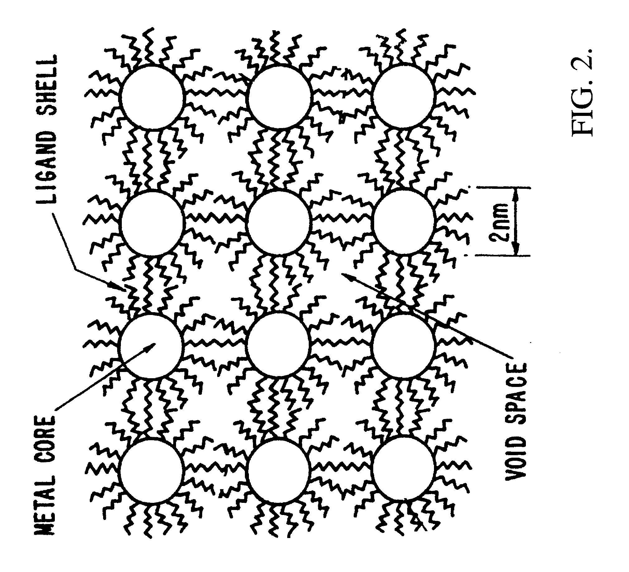
The present invention is a chemiresistor for qualitative and quantitative analysis of chemical species that consists of a very thin film of particles, nanoclusters, deposited on an insulating substrate and contacted by electrodes. The particles have a metallic core, preferably spheroidal, that is less than 5 nm in diameter and surrounded by an monolayer ligand shell ranging in thickness from 0.4 nm to 2 nm. The Coulomb blockade effects upon which the invention operates result in nonlinear current-voltage characteristics which dramatically improves sensitivity with much lower power dissipation. One property of the ligand shell is that its chemical composition can be chosen to be especially receptive to a particular chemical vapor.

Description

[0001] 1. Field of the Invention[0002] This invention relates to chemical sensing devices and, more specifically, to the qualitative and quantitative analysis of a chemical species in a target environment wherein the properties of certain nanoclusters interact with the chemical species such that they can be monitored as an indication of whether the species is present and in what amount.[0003] 2. Description of the Background Art[0004] There are a number of well-known approaches for determining the presence and amount of a chemical species in a target environment by exposing a substance capable of interacting with the species to such environment and monitoring a change in a property of that substance due to such interaction as an indication of whether or in what amount the species is present.[0005] One such approach has been the exposure to the environment of a species-interactive substance applied to a piezoelectric substrate. The substance is affected such that, if any of the speci...

Claims


Application Information

Patent Timeline
IPC IPC(8): G01N27/04
CPCB82Y10/00B82Y15/00Y10T436/18G01N27/127Y10T436/173845B82Y30/00
Inventor SNOW, ARTHURANCONA, MARIOFOOS, EDWARD
Owner THE UNITED STATES OF AMERICA AS REPRESENTED BY THE SECRETARY OF THE NAVY
Learn More