DNA-bridged carbon nanotube arrays
a carbon nanotube and array technology, applied in the field of biological sensing devices, can solve the problems of poor specificity and reproducibility, long recovery time, and prior art probes, and achieve the effects of optimizing sensitivity, high degree of accuracy, and significantly elevated conductivity
- Summary
- Abstract
- Description
- Claims
- Application Information
AI Technical Summary
Benefits of technology
Problems solved by technology
Method used
Image
Examples
example 2
[0102] Growth of Controlled Dimension Gold-Coated Spheres
[0103] Gold-coating procedure of spheres utilizes the functionalization of microspheres with thiols groups to enable the self-assembly of metallic gold nanoparticles on functionalized sphere surfaces. The initially formed gold layer is subsequently built up either through sequential steps of linker addition followed by additional contact with gold nanoparticles, or through electroless deposition of gold on the functionalized sphere surfaces.
example 3
[0104] Synthesis of DNA Sequences with Thiol Linkers
[0105] The synthetic method involves a solution-phase reaction between 4-mercaptobenzoic acid and a terminal amine either at the 2' or 5' position on the ribose moiety. The incorporation of an amine at the 2' or 5' position is accomplished during chemical DNA synthesis using commercially available reagents. A 2'-derivatization is carried out to orient the DNA away from a gold surface when the linker is placed at the 3' end of an oligonucelotide, while a 5'-derivization is done to orient the oligonucleotide linked at the 5' end. Alternatively 4-mercaptobenzoic acid is reacted with a 5' pendant alkyl-amine or the incorporation of a short alkanethiol linker to the 3' end of DNA using a commercially-available reagent.
example 4
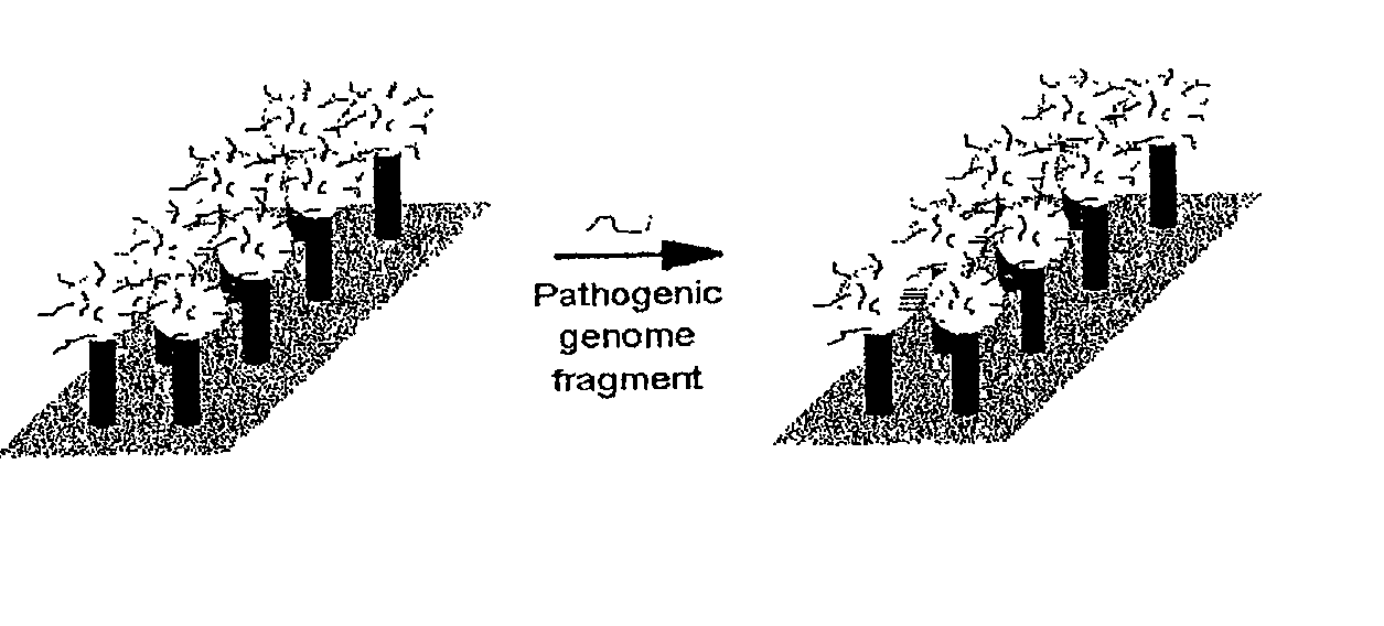
[0106] Fabrication of Electrically-Addressable Carbon Nanotube Arrays
[0107] The preliminary step involves a micro- and nanolithographic preparation of CNT catalyst sites and metallic addressing wires on single crystal silicon wafers. This is followed by growth of aligned CNTs via hot filament, plasma-enhanced chemical vapor deposition (PECVD). A series of thin gold wires lithographically on the silicon is defined, with the inner ends of pairs of individual wires in very close proximity (.about.100 nm). At these proximal ends, a CNT growth catalyst (e.g., Ni or Co) nanodot site is defined using e-beam lithography, and the catalyst material deposited. This wafer is then placed in the CVD chamber, with subsequent CNT growth occurring only at the catalyst nucleation sites. At this point the gold wires may be passivated using electropolymerization. If deemed necessary, additional steps can be introduced to obtain strictly uniform height of the CNTs in the arrays. Depending on growth cond...
PUM
| Property | Measurement | Unit |
|---|---|---|
| Electrical conductivity | aaaaa | aaaaa |
| Electric charge | aaaaa | aaaaa |
| Electrical conductor | aaaaa | aaaaa |
Abstract
Description
Claims
Application Information
 - R&D
- Intellectual Property
- Life Sciences
- Materials
- Tech Scout
- Unparalleled Data Quality
- Higher Quality Content
- 60% Fewer Hallucinations
Browse by: Latest US Patents, China's latest patents, Technical Efficacy Thesaurus, Application Domain, Technology Topic, Popular Technical Reports.
© 2025 PatSnap. All rights reserved.Legal|Privacy policy|Modern Slavery Act Transparency Statement|Sitemap|About US| Contact US: help@patsnap.com


