Optoelectronic substrate

Inactive Publication Date: 2002-11-14
CANON KK
View PDF18 Cites 56 Cited by
  • Summary
  • Abstract
  • Description
  • Claims
  • Application Information

AI Technical Summary

Benefits of technology

[0022] The waveguide characteristics and the optical coupling characteristics can be controlled by designing suitably the repeating period and the like of the photonic crystal, and thereby the freedom degree in designing the optical circuit like routing can be increased.
[0024] In this second embodiment, the anodized alumina insulates electrically the electric devices and the optical devices mounted thereon, and serves as an optical wiring and an optical coupler, whereby the optoelectronic wiring device can be made compact by a simple technique, and further the electromagnetic emission noise can be reduced, enabling high-speed data processing with high reliability.
[0026] Further, the heat releasing ability of the optoelectronic wiring substrate can be improved by placing the anodized alumina on a metal base plate such as an aluminum plate. Filling of the anodized alumina holes with an electroconductive material makes the anodized alumina useful as an electric wiring for connecting electrically the electronic devices or the optical devices.
[0027] Filling of the anodized alumina holes with a magnetic material makes the anodized alumina useful as an electromagnetic wave absorber, which gives an optoelectronic wiring substrate less sensitive to electromagnetic emission noise. Thus by placing suitably the filled anodized alumina, electromagnetic interference caused by the electromagnetic emission noise can be reduced.
[0028] Furthermore, the anodized alumina can be produced in a large area readily at a low cost, advantageously.

Problems solved by technology

However, with increase of the processing speed, the adverse effect of wiring delay has become remarkable.
However, the increase of the processing speed has given rise to another problem of electromagnetic radiation interference noise (EMI).
Consequently, when signals flow in a high speed through adjacent wirings, the electromagnetic waves can interfere with each other to cause noises, preventing precise transmission of the signals.
In particular, in mobile terminals, which are coming to be driven at a lower voltage and higher electric current intensity, the adverse effect of the EMI is becoming serious.
However, this is not satisfactory in the production cost and yield.
Therefore, entire change of the electric wiring to the optical wiring causes increase of the size or increase of the loss by bending disadvantageously.
Further, introduction of the optical wiring requires change of the electric wiring pattern disadvantageously.
Such methods, however, has disadvantage in yield and equipment cost in patterning.
In recent years, heat removal from the devices is becoming an important problem with increase of the frequency of the electronic circuit, and increase of the speed and density of the signals.
Accumulation of the generated heat may degrade the device properties, or may damage the electronic part.

Method used


Image

  • Optoelectronic substrate
  • Optoelectronic substrate
  • Optoelectronic substrate

Examples


example 1

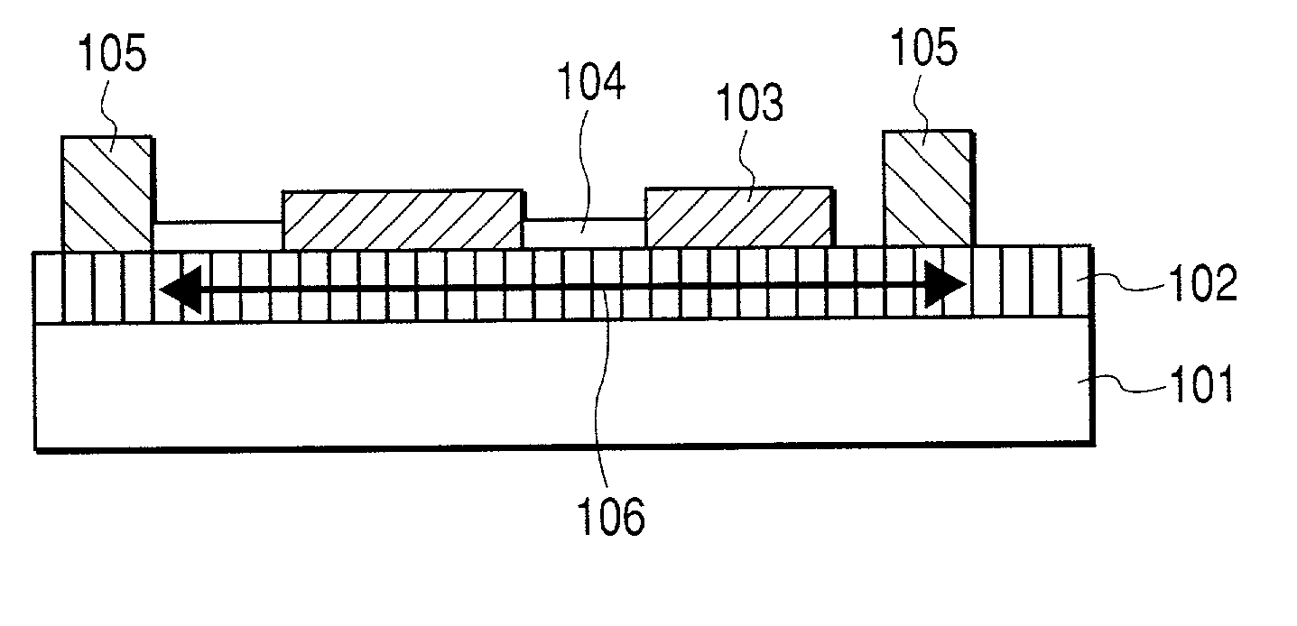
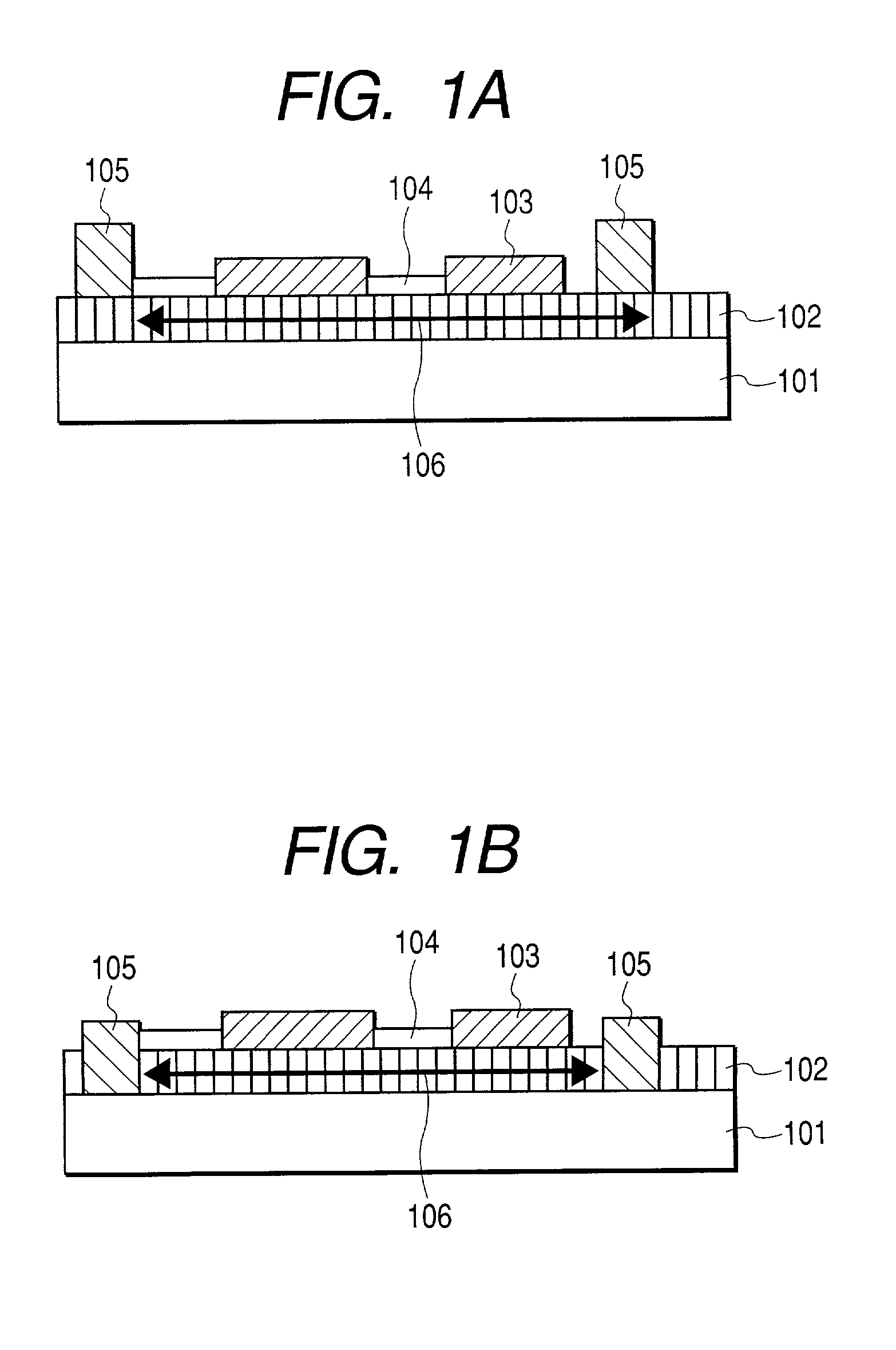
[0144] In this Example, anodized alumina was formed on an aluminum plate, and thereon an electric device and an optical device were mounted as illustrated in FIGS. 1A and 1B.

[0145] Firstly, on an aluminum plate, anodized alumina 102 was formed in a thickness of 5 .mu.m. The remaining unanodized portion serves as base plate 101.

[0146] Prior to the anodization, hole-starting points (concaves) were formed on the surface of the aluminum plate by FIB irradiation. This enables the holes regularly arranged in a honeycomb state (triangular lattice state). In this example, a focused ion beam of Ga was projected to form hole-starting points in dots arranged in 360 nm intervals in triangular lattice arrangement, with ion species of Ga, at acceleration voltage of 30 kV, ion beam diameter of 100 nm, ion current of 300 pA, and irradiation time for each dot of 10 msec.

[0147] The anodization was conducted with an apparatus illustrated in FIG. 11, in a 0.3M phosphoric acid bath as the anodization el...

example 2

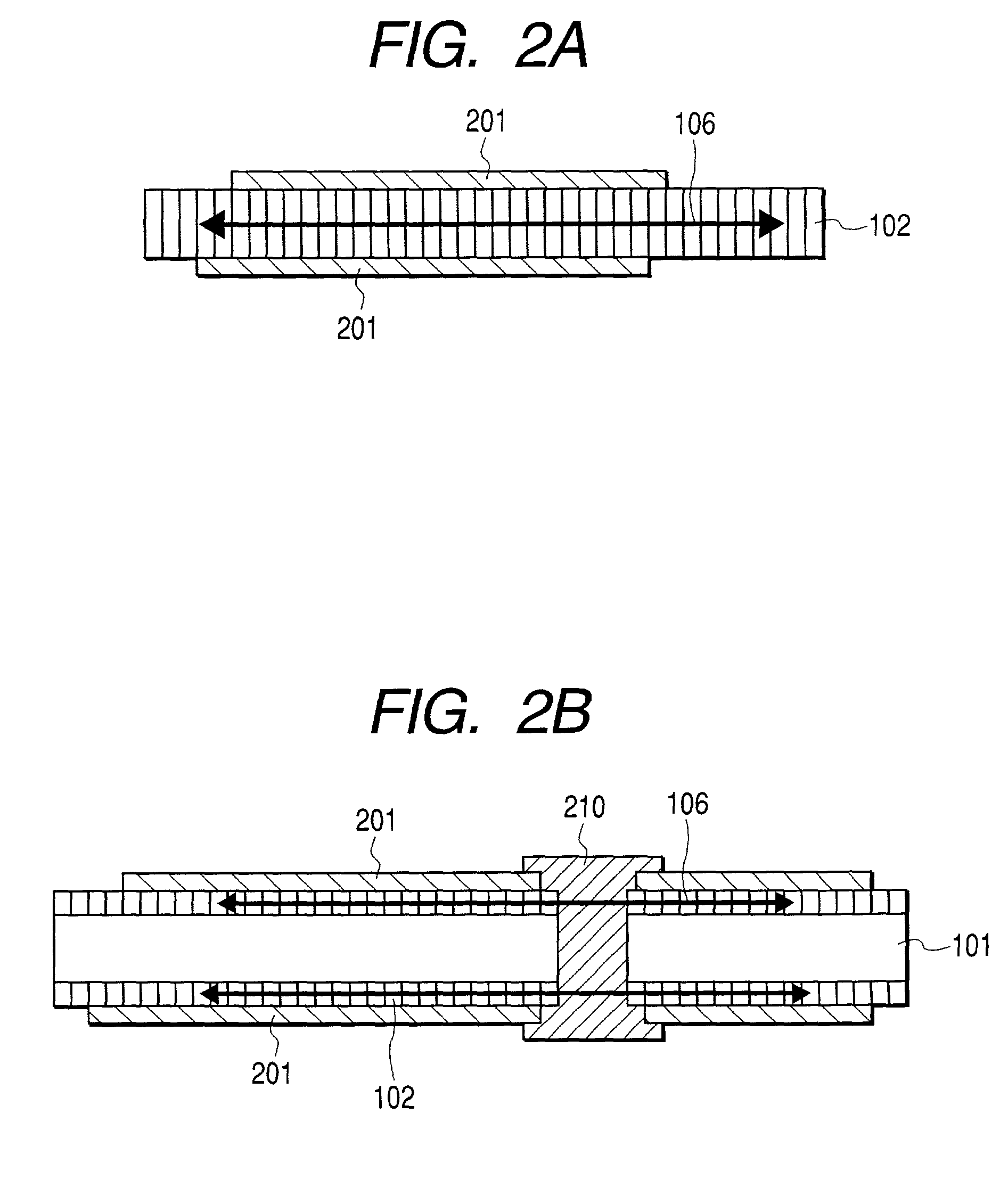
[0153] In this Example, anodized alumina itself was used as the base plate as illustrated in FIG. 4B, and a device was provided on each of the upper and lower faces respectively, and some of the holes were utilized as via holes to connect electrically and optically the devices on the both faces.

[0154] Anodized alumina was fabricated in the same manner as in Example 1.

[0155] Anodization was conducted in a 0.3 M phosphoric acid solution bath as the electrolyte solution at an anodization voltage of 88 V. Further, a hole-widening treatment was conducted by immersion in a 5 wt % phosphoric acid solution for 40 minutes to obtain anodized alumina of hole intervals of 220 nm and hole diameter of about 100 nm. The remaining aluminum was dissolved by an aqueous mercury chloride to isolate the anodized alumina.

[0156] Subsequently, PMMA (poly-methyl-methacrylate) was filled into the holes to form a waveguide pattern. In this Example, the PMMA-filled holes serve as the waveguide as shown in FIG....

example 3

[0160] In this Example, Fe was filled into fine holes of anodized alumina 102 to have a function of electromagnetic wave absorber 501 as shown in FIG. 5B. In this drawing, the magnetic material was filled into a part of thickness of the holes. Naturally, the magnetic material may be filled into the entire of the holes in the thickness direction, or may be filled only into the holes to be employed as the electromagnetic wave absorber.

[0161] Firstly, an Nb film, and an aluminum film were formed on an Si base plate. The aluminum film was converted to anodized alumina.

[0162] The anodized alumina was adjusted to have a thickness of 5 .mu.m, hole spacings of 300 nm, and hole diameters of 100 nm. Into the holes of the anodized alumina, Fe was filled to a depth of about 1 .mu.m by electrodeposition.

[0163] On the anodized alumina, an electric wiring was formed with electroconductive paste, and electronic devices and optical devices were mounted to obtain an optoelectronic wiring substrate. A...


PUM


Abstract

An optoelectronic substrate comprises an electronic device, an optical device, and an optical wiring layer, the optical wiring layer comprising a photonic crystal. An optoelectronic substrate comprises an electronic device, an optical device, and an optical wiring layer, wherein the optical wiring layer is comprised of a periodic structure having a repeating period nearly equal to or smaller than the wavelength of light employed for signal transmission. An optoelectronic substrate comprises an electronic device, an optical device, an electric wiring connected to the electronic device, an optical wiring layer, and a base plate, wherein the optical wiring layer is employed as an insulating layer between the base plate and the electric wiring.

Description

BACKGROUDN OF THE INVENTION[0001] 1. Field of the Invention[0002] The present invention relates to an optoelectronic substrate, particularly to a circuit substrate having an electronic device and an optical device in combination.[0003] 2. Related Background Art[0004] In recent years, data processing apparatuses such as portable telephones and personal digital assistance (PDA) are required to have a high-speed processing ability, a small size, and a light weight simultaneously. However, with increase of the processing speed, the adverse effect of wiring delay has become remarkable. To prevent the wiring delay, the simplest way is to shorten the wirings inside and between the chips. The wire-shortening is also helpful in miniaturizing the substrate, so that many inventions have been disclosed thereon.[0005] However, the increase of the processing speed has given rise to another problem of electromagnetic radiation interference noise (EMI).[0006] The problem of EMI is explained below.[...

Claims


Application Information

Patent Timeline
IPC IPC(8): G02B6/122G02B6/13G02B6/34G02B6/42G02B6/43H05K1/02H05K1/05
CPCB82Y20/00G02B6/1225G02B6/13G02B6/34H05K1/053G02B6/4277G02B6/43H05K1/0274G02B6/42
Inventor IWASAKI, TATSUYADEN, TORU
Owner CANON KK
Why Eureka
Try Eureka