
Electrode for use in electro-optical devices

Inactive Publication Date: 2002-09-19
AU OPTRONICS CORP
View PDF0 Cites 96 Cited by
  • Summary
  • Abstract
  • Description
  • Claims
  • Application Information

AI Technical Summary

Benefits of technology

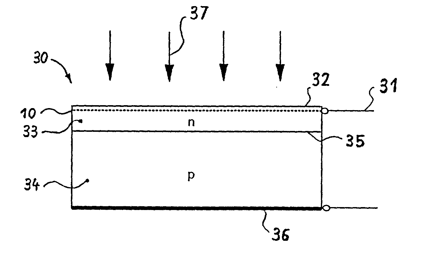
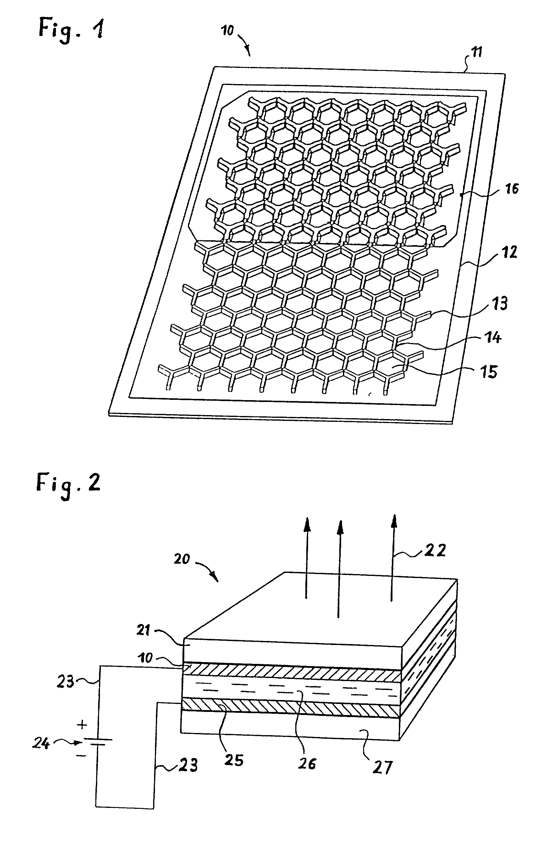
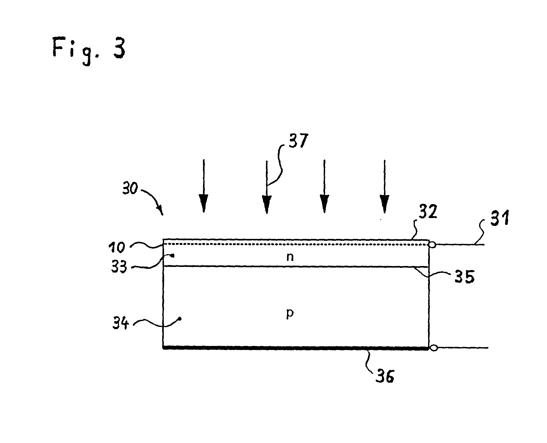
[0019] Due to the small geometry of the elements, which can be straps or spheres or combinations thereof, Mie scattering occurs, making the electrode appear transparent for a certain wavelength range. It is an advantage of the present invention that the transparency of such an electrode is very high, because some incidence of light on the small elements will be forward scattered and no longer reflected backwards as aforementioned. The total percentage of coverage caused by conductive elements is low and the power distribution is very high compared to today's solutions. The present invention provides the ability to make displays and all other electro-optical devices with better performance. In the following the electrode according to the present invention will also be referred to as transparent electrode.
[0020] The elements comprise a suited material, such as metal, an alloy, semiconductor or a conductive polymer to guarantee for a good conductivity. It should be noted that the word electrode herein used is meant to cover the conductive elements and the spaces, because the spaces together with the conductive elements influence the electrode's properties. Furthermore, the conductive elements are arranged in form of a regular pattern or structure and have a size and a geometry which might determine the direction of the light. The geometry of the electrode, that means the pattern of conductive elements is highly application specific. For instance, optical effects like polarization and viewing angle adjustments are achievable. An enhancement will be achieved if the electrode is designed appropriately. The redundancy of the structure of the elements, which will electrically compensate broken elements or straps, is a huge advantage for every production process.
[0021] The conductive elements of the inventive electrode has a surface coverage of about 1% to 20% and preferably less than 11% or even less than 6%. Because of the forward scattered light, the loss of light will be less than the values mentioned before. This will provide more transparency compared to common electrodes. Less energy is necessary and therefore portable battery-powered applications can be used for a longer time.
[0022] A resistance of about 0.01 .OMEGA. / .quadrature. to 100 .OMEGA. / .quadrature., preferably less than 1 .OMEGA. / .quadrature., can be achieved. For purposes of the present invention the term "ohms per square (.OMEGA. / .quadrature.)" is used to designate sheet resistivity over a given surface area in a conventional manner.
[0023] The electrode has a topside modifier and a backside modifier. In the following, topside modifier and backside modifier together will be called modifiers. The modifiers are optional. The modifiers can be built of any suited material. Their structure depends on the application. It is an advantage of the electrode according to the present invention that modifier(s) can be employed. For example
[0024] the modifiers are made of SiO.sub.x which can have protecting functions; or

Problems solved by technology

However, the TCO films in practical use for these devices still have several unsolved problems such as high cost, low transparency, and poor conductivity.
Another disadvantage of the state of the art is that usual electrodes are not absolutely invisible and cover a large portion of an electro-optical device.

Method used


Image

  • Electrode for use in electro-optical devices
  • Electrode for use in electro-optical devices
  • Electrode for use in electro-optical devices

Examples


Embodiment Construction

[0040] Before embodiments of the present invention are described, the basic elements, in accordance with the present invention, are addressed.

[0041] Electrode:

[0042] An electrode is a component of an electric circuit that connects the conventional wiring of a circuit to a conducting medium. The electrically positive electrode is called the anode and the negative electrode is called the cathode. As aforementioned the electrode of the present invention includes conductive elements and spaces between the conductive elements.

[0043] The Mie effect:

[0044] The Mie theory for a sphere provides the only practical method for calculating light-scattering properties of finite particles of arbitrary size and refraction index. The scattering theory does provide also a first-order description of optical effects in nonspherical particles, and it correctly describes many small-particle effects that are not intuitively obvious.

[0045] Excluding the case where the conductivity or the dielectric constan...


PUM


Abstract

An electrode for an electro-optical device is provided. Light is passing through this electrode which comprises a pattern of conductive elements. The elements have dimensions small compared to the wavelength of light, so that the electrode appear transparent. The light intensity distribution after having penetrated the electrode compared with the light intensity distribution before having penetrated the electrode is influenced by forward scattering.

Description

BACKGROUND OF THE INVENTION[0001] 1. Technical Field[0002] The present invention concerns an electrode. More particularly, the invention relates to an electrode for use in electro-optical devices, such as displays or solar cells.[0003] 2. Prior Art[0004] Many different kinds of electrodes are known. About electrodes for electro-optical applications and devices have been reported widely in recent years. Of particular interest is the electrical and optical characteristics of such electrodes.[0005] U.S. Pat. No. 4,518,891 to Howard, Jr. discloses large area electroluminescent (EL) faceplates for a storage cathode ray tube (CRT). It describes a macroscopic metallic mesh to hold the electrical potential constant.[0006] Another metal structure called metal assist structure is disclosed in U.S. Pat. No. 5,455,899 to Budzilek et al., which is related to electroluminescent devices in general.[0007] U.S. Pat. No. 5,131,065 to Briggs et al. discloses an optically enhanced flat display panel. I...

Claims


Application Information

Patent Timeline
IPC IPC(8): G09F9/30G02F1/1343H01L31/0224H01L31/04H01L33/38H01L51/52
CPCB82Y10/00B82Y30/00G02F1/13439H01J2211/225H01L31/022408H01L31/022425H01L31/022433H01L33/38H01L51/5203Y02E10/50H10K59/805H10K50/805
Inventor MUELLER, PETERRIESS, WALTER
Owner AU OPTRONICS CORP
Learn More