
Process for the surface polishing of silicon wafers

Inactive Publication Date: 2002-06-20
SILTRONIC AG
View PDF0 Cites 108 Cited by
  • Summary
  • Abstract
  • Description
  • Claims
  • Application Information

AI Technical Summary

Benefits of technology

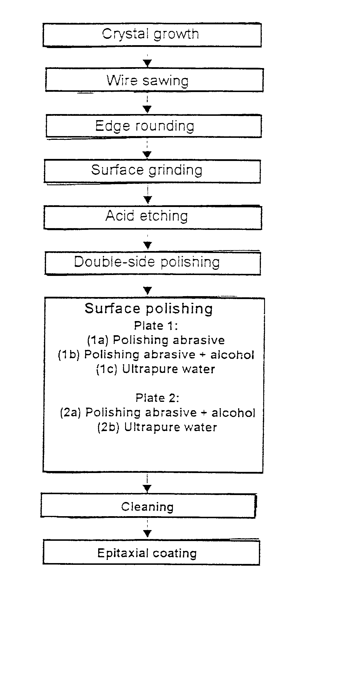
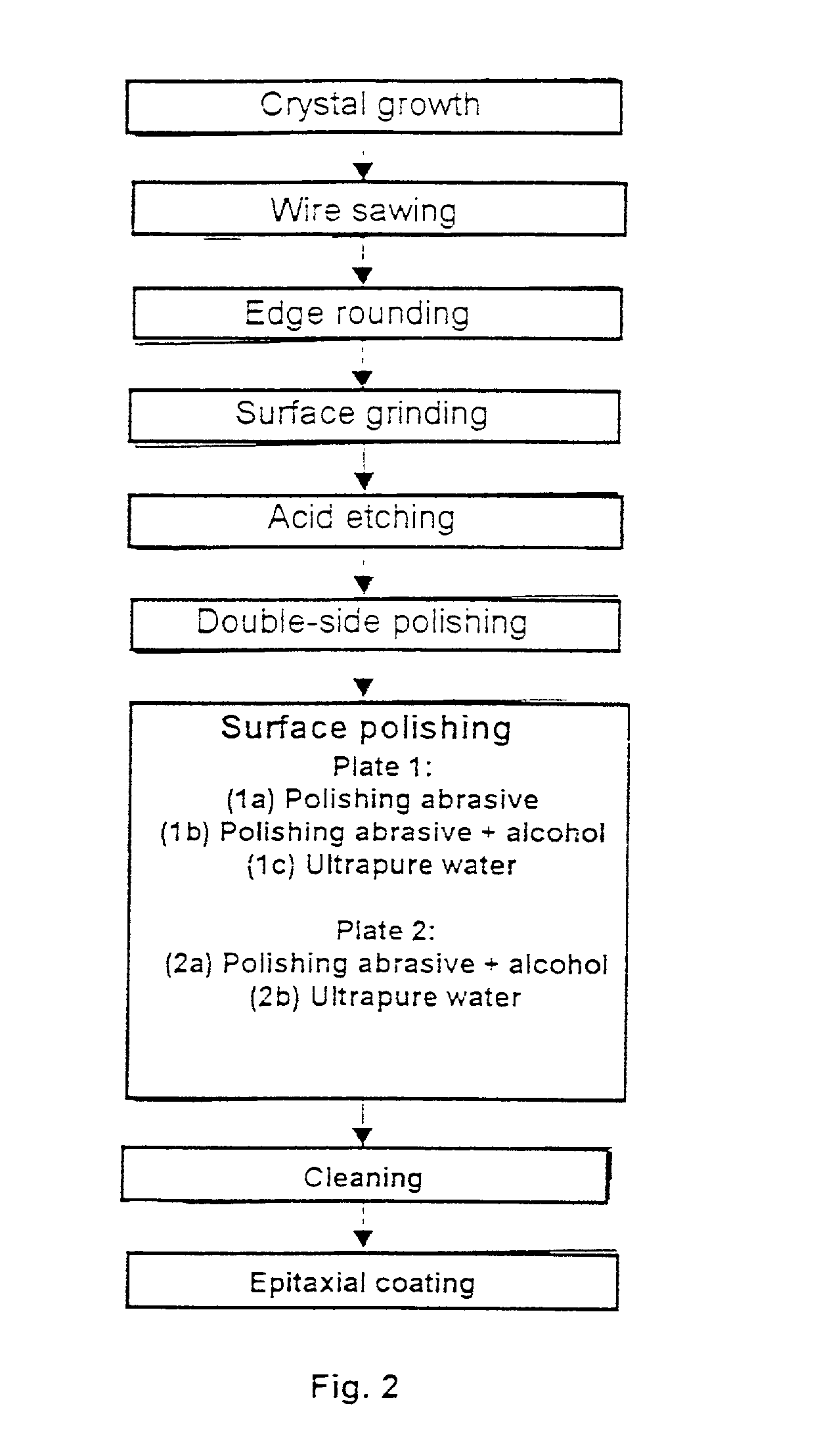
[0012] An essential feature of the invention is that the improved surface-polishing process has a mixture of polishing abrasive and alcohol being added to both polishing plates. This leads to a significant reduction in localized light scatterers, in particular of stacking faults, on an epitaxial coating applied to this surface, compared to processes according to the prior art. The present invention leads to higher yields and therefore lower costs during the fabrication of semiconductor components. This was unexpectedly surprising and impossible to predict.
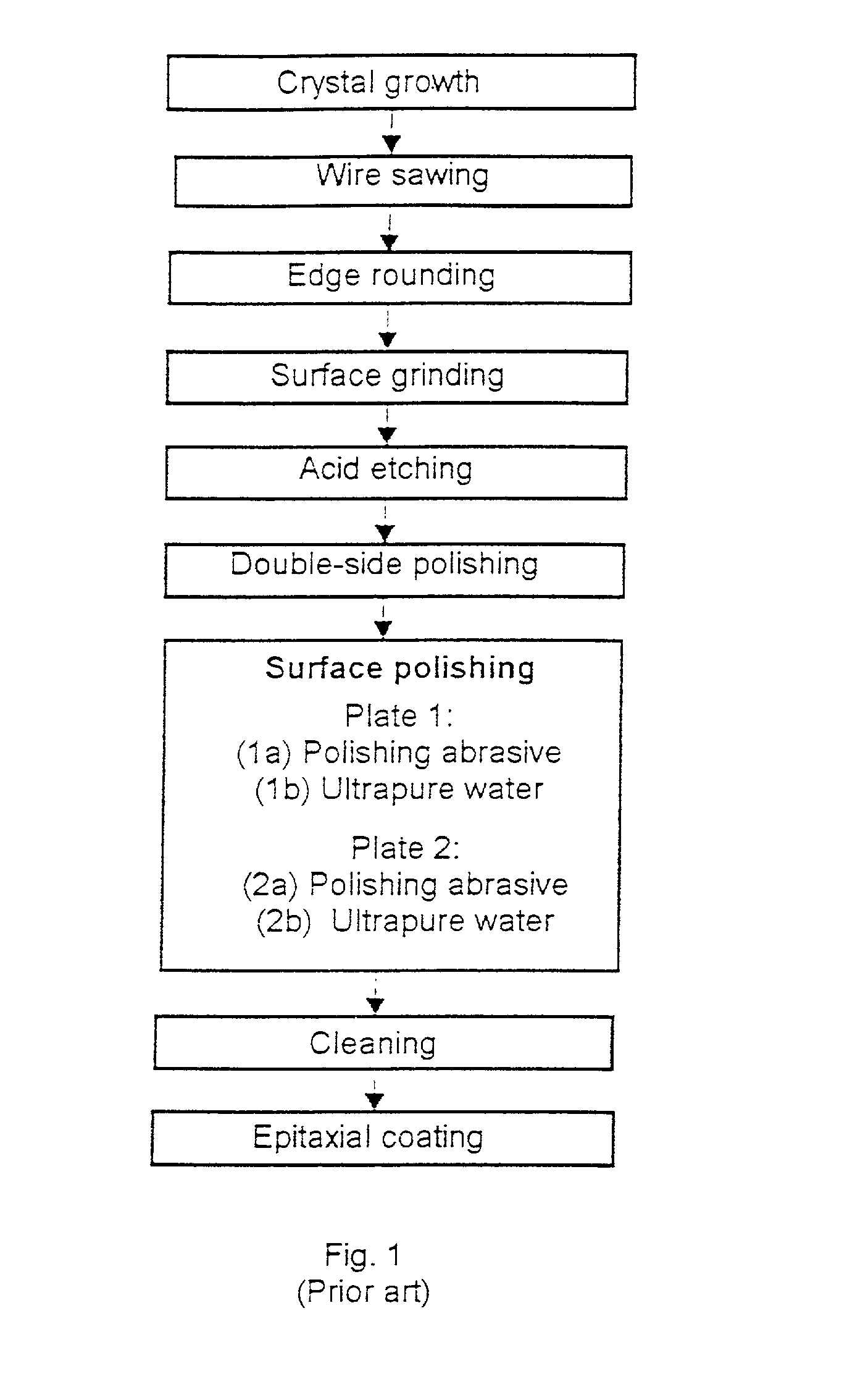
[0016] To improve the geometry and partially remove damage, it is possible for the silicon wafers to be subjected to a mechanical abrasion step, such as lapping or grinding. This is done in order to reduce the amount of material which has to be removed in the stock-removal polishing step. Both processes are equally preferred. When carrying out a grinding process, it is particularly preferable for the two sides to be ground sequentially or simultaneously. To remove damage from the wafer surface and edge and to eliminate in particular metallic impurities, an etching step is preferred at this point. This etching step may particularly preferably be carried out as a wet-chemical treatment of the silicon wafer in an alkaline or acidic etching mixture, with the removal of from 1 to 50 .mu.m of silicon.

Problems solved by technology

In this single-side surface polishing, a suitable combination of polishing abrasive and polishing cloth usually leads to significantly lower material removal rates than stock-removal polishing processes.
However, the surface-polishing processes according to the prior art lead to silicon wafers which, following an epitaxial coating, have a certain number of surface defects which cannot be cleaned off.
For example stacking faults and other localized light scatterers, which are detected by laser measurement in the size range of, for example, over 0.12 .mu.m and, on account of electric short circuits, can lead to failures during the component fabrication process.
This was unexpectedly surprising and impossible to predict.

Method used


Image

  • Process for the surface polishing of silicon wafers
  • Process for the surface polishing of silicon wafers
  • Process for the surface polishing of silicon wafers

Examples


example

Invention

[0036] The procedure utilized was analogous to that used in the Comparative Example. The following procedure was selected for the surface polishing, with the same polishing cloths being used. First of all, on plate 1, polishing was once again carried out with LEVASIL 300.RTM. (3% by weight of SiO.sub.2; pH 10.5), this time for 120 sec. Then, a polishing abrasive which comprised an aqueous suspension of pyrogenic silica (SiO.sub.2 particle size 30-40 nm; solid content 1.5% by weight; NH.sub.4OH-stabilized), to which 0.2% by volume of triethylene glycol had been admixed and which had a pH of 9.7, was added for 40 sec. Then, ultrapure water was supplied for 20 sec. On plate 2, with an otherwise identical procedure to that utilized in the Comparative Example, the same suspension of pyrogenic silica with added triethylene glycol as on plate 1 was used. The total amount of silicon removed from the front surface of the silicon wafer was this time on average 0.5 .mu.m, of which app...


PUM

PropertyMeasurementUnit
Percent by massaaaaaaaaaa

Abstract

A process for the surface polishing of a silicon wafer, includes the successive polishing of the silicon wafer on at least two different polishing plates covered with polishing cloth, with a continuous supply of alkaline polishing abrasive with SiO2 constituents, an amount of silicon removed during the polishing on a first polishing plate being significantly higher than on a second polishing plate, with the overall amount of silicon removed not exceeding 1.5 mum. A polishing abrasive (1a), then a mixture of a polishing abrasive (1b) and at least one alcohol, and finally ultrapure water (1c) are added to the first polishing plate, and a mixture of a polishing abrasive (2a) and at least one alcohol and then ultrapure water (2b) are added to the second plate.

Description

[0001] 1. Field of the Invention[0002] The present invention relates to a process for producing a silicon wafer with a back surface and a front surface which has been polished until it is free of haze. This wafer is suitable for use in the semiconductor industry, in particular for the fabrication of electronic components following the application of an epitaxial coating.[0003] 2. The Prior Art[0004] According to the prior art, silicon wafers for use in the semiconductor industry are produced by sawing up a silicon single crystal, followed by edge rounding, lapping or grinding, wet-chemical etching, polishing and cleaning. The polishing has two essential roles. The first is that of producing the ultimate planarity which is required in order to avoid focusing problems for the stepper during component fabrication, firstly, and a low-defect surface. The second, on which--if appropriate after the application of an epitaxial coating--the failure of semiconductor components caused by elect...

Claims


Application Information

Patent Timeline
IPC IPC(8): B24B37/00B24B37/04C09K3/14H01L21/304H01L21/306
CPCH01L21/02024H01L21/304
Inventor WENSKI, GUIDOBUSCHHARDT, THOMASHENNHOFER, HEINRICHLICHTENEGGER, BRUNO
Owner SILTRONIC AG
Learn More